
5SGXMB6R1F40I2N
| Part Description |
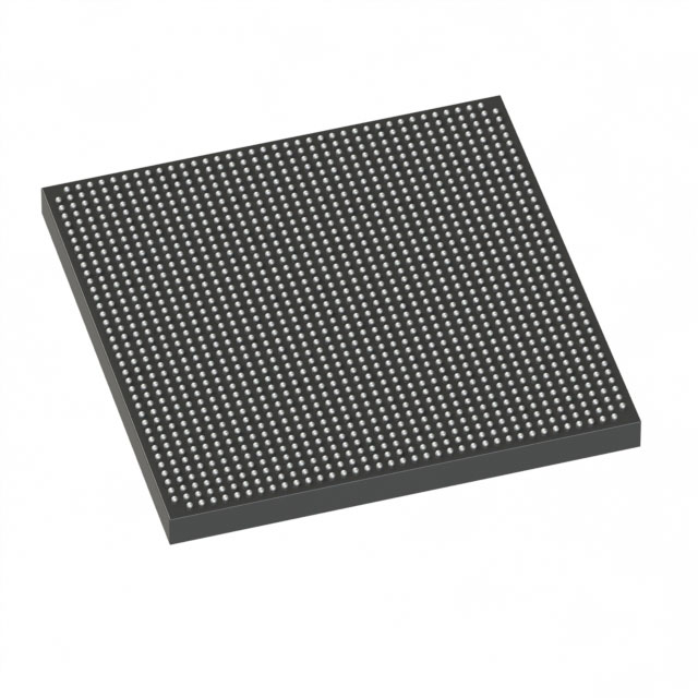
Stratix® V GX Field Programmable Gate Array (FPGA) IC 432 53248000 597000 1517-FBGA (40x40) |
|---|---|
| Quantity | 987 Available (as of June 15, 2026) |

| Product Category | Field Programmable Gate Array (FPGA) |
|---|---|
| Manufacturer | Intel |
| Manufacturing Status | Obsolete |
| Manufacturer Standard Lead Time | Contact Us |
| Datasheet |
Specifications & Environmental
| Device Package | 1517-FBGA (40x40) | Grade | Industrial | Operating Temperature | -40°C – 100°C | ||
|---|---|---|---|---|---|---|---|
| Package / Case | 1517-FBGA (40x40) | Number of I/O | 432 | Voltage | 870 mV - 930 mV | ||
| Mounting Method | Surface Mount | RoHS Compliance | RoHS Compliant | REACH Compliance | REACH Unknown | ||
| Moisture Sensitivity Level | 3 (168 Hours) | Number of LABs/CLBs | 225400 | Number of Logic Elements/Cells | 597000 | ||
| Number of Gates | N/A | ECCN | 3A001A2C | HTS Code | 8542.39.0001 | ||
| Qualification | N/A | Total RAM Bits | 53248000 |
Overview of 5SGXMB6R1F40I2N – Stratix® V GX Field Programmable Gate Array (FPGA)
The 5SGXMB6R1F40I2N is an Intel Stratix® V GX family FPGA in a 1517‑FBGA (40×40) surface‑mount package, offered in an industrial temperature grade. This device provides a high-density fabric with substantial embedded memory and a large I/O complement for complex digital designs.
With 597,000 logic elements, approximately 53.25 Mbits of on‑chip RAM and 432 I/O pins, this device is targeted at system designs that require large programmable logic capacity, significant embedded memory, and broad external connectivity while operating across an industrial temperature range.
Key Features
- High logic capacity — 597,000 logic elements provide extensive programmable resources for complex logic, datapath, and control implementations.
- Large embedded memory — Approximately 53.25 Mbits of on‑chip RAM to support buffering, FIFOs, and distributed memory needs within the FPGA fabric.
- Extensive I/O — 432 dedicated I/O pins to interface with multiple peripherals, high‑speed buses, and external devices.
- Fabric granularity — 225,400 logic cells (LAB/CLB equivalent) offering fine‑grained implementation options for custom logic and IP integration.
- Industrial grade — Rated for operation from −40 °C to 100 °C to meet demanding environmental requirements for industrial deployments.
- Core voltage — Operates from 870 mV to 930 mV, enabling designers to plan accurate power delivery and thermal management for core supply rails.
- Package and mounting — 1517‑FBGA (40×40) surface‑mount package for high‑density board integration.
- RoHS compliant — Meets RoHS requirements for lead‑free assembly and environmental compliance.
Typical Applications
- High‑performance signal processing — Large logic capacity and embedded RAM enable complex DSP pipelines, filtering, and protocol processing.
- Network and communications — High I/O count supports interfacing to multiple transceivers, PHYs, and external packet processing logic.
- Data acceleration and custom compute — Dense logic resources and on‑chip memory make the device suitable for hardware acceleration and custom compute functions.
- Industrial control and automation — Industrial temperature rating and extensive I/O allow deployment in rugged control, monitoring, and interface applications.
Unique Advantages
- Scalable logic density: 597,000 logic elements let you consolidate functions that would otherwise require multiple devices, reducing BOM and board complexity.
- Integrated memory bandwidth: Approximately 53.25 Mbits of embedded RAM reduces external memory dependence and accelerates on‑chip data paths.
- Broad external connectivity: 432 I/O pins provide flexibility to connect a wide range of peripherals and high‑pin‑count interfaces without external multiplexing.
- Industrial robustness: −40 °C to 100 °C operating range supports deployment in industrial environments with wide temperature swings.
- Compact packaging: 1517‑FBGA (40×40) surface‑mount package supports high‑density PCB layouts while maintaining extensive I/O and logic resources.
- Compliance readiness: RoHS compliance aligns with modern assembly and environmental requirements.
Why Choose 5SGXMB6R1F40I2N?
The 5SGXMB6R1F40I2N combines a high logic element count, substantial on‑chip memory, and a large I/O complement in an industrial‑grade Stratix V GX FPGA package. It is well suited for engineers and system designers who need high-density programmable logic with robust environmental performance and strong on‑chip memory resources.
This device is a fit for designs that require consolidation of complex logic blocks, reduced external memory dependence, and extensive peripheral interfacing—providing a balance of integration and deployment readiness for industrial and high‑performance applications.
Request a quote or submit an RFQ to begin procurement and receive availability and pricing information for 5SGXMB6R1F40I2N. Technical inquiries and volume requests are welcome to help determine fit for your design.


Date Founded: 1968
Headquarters: Santa Clara, California, USA
Employees: 130,000+
Revenue: $54.23 Billion
Certifications and Memberships: ISO9001:2015, ISO14001:2015, ISO17025:2017, ISO27001:2022, ISO45001:2018, ISO50001:2018


