
5SGXMB6R1F43C2LN
| Part Description |
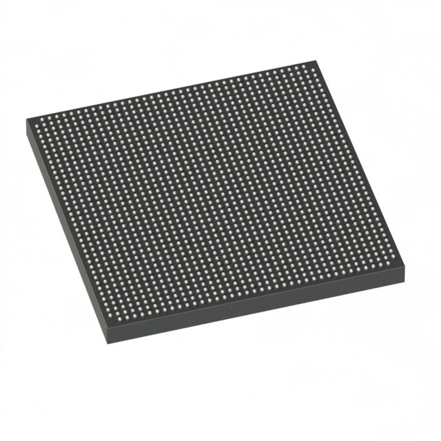
Stratix® V GX Field Programmable Gate Array (FPGA) IC 600 53248000 597000 1760-BBGA, FCBGA |
|---|---|
| Quantity | 197 Available (as of June 14, 2026) |

| Product Category | Field Programmable Gate Array (FPGA) |
|---|---|
| Manufacturer | Intel |
| Manufacturing Status | Obsolete |
| Manufacturer Standard Lead Time | Contact Us |
| Datasheet |
Specifications & Environmental
| Device Package | 1760-FCBGA (42.5x42.5) | Grade | Commercial | Operating Temperature | 0°C – 85°C | ||
|---|---|---|---|---|---|---|---|
| Package / Case | 1760-BBGA, FCBGA | Number of I/O | 600 | Voltage | 820 mV - 880 mV | ||
| Mounting Method | Surface Mount | RoHS Compliance | RoHS Compliant | REACH Compliance | REACH Unknown | ||
| Moisture Sensitivity Level | 3 (168 Hours) | Number of LABs/CLBs | 225400 | Number of Logic Elements/Cells | 597000 | ||
| Number of Gates | N/A | ECCN | 3A001A2C | HTS Code | 8542.39.0001 | ||
| Qualification | N/A | Total RAM Bits | 53248000 |
Overview of 5SGXMB6R1F43C2LN – Stratix V GX FPGA; 597,000 logic elements, ~53 Mbits RAM, 600 I/Os, 1760‑FCBGA
The 5SGXMB6R1F43C2LN is a Stratix® V GX field programmable gate array (FPGA) from Intel, offered in a 1760‑FBGA surface‑mount package. This commercial‑grade device provides a very large logic fabric and substantial on‑chip memory suitable for high‑density, configurable digital designs.
With 597,000 logic elements, approximately 53 Mbits of embedded RAM and 600 I/O pins, the device is targeted at applications that require large programmable logic capacity, extensive I/O connectivity and a compact 1760‑FCBGA footprint. The device follows the Stratix V family electrical and switching characteristics detailed in the device datasheet.
Key Features
- Logic Capacity 597,000 logic elements and 225,400 CLBs provide very large programmable logic resources for complex designs.
- Embedded Memory Approximately 53 Mbits of on‑chip RAM to support buffering, LUT storage and memory‑intensive logic tasks.
- I/O Density 600 I/O pins accommodate extensive peripheral, interface and signaling requirements without external multiplexing.
- Package and Mounting 1760‑FCBGA package (42.5 × 42.5 mm) with surface‑mount construction for high‑density board implementations.
- Power Supply Core supply voltage range specified from 820 mV to 880 mV for the device core.
- Temperature Rating Commercial operating temperature range of 0 °C to 85 °C for standard environmental deployments.
- Stratix V GX Family Characteristics Device is part of the Stratix V GX family; refer to the Stratix V device datasheet for family electrical, switching and transceiver speed‑grade details.
- RoHS Compliance RoHS‑compliant device suitable for standard commercial manufacturing flows.
Typical Applications
- High‑density programmable logic systems — Systems that require hundreds of thousands of logic elements and significant embedded RAM can be implemented on this device.
- I/O‑intensive designs — Applications needing a large number of external interfaces benefit from the device’s 600 I/O pins.
- Embedded memory‑dependent logic — Designs that rely on substantial on‑chip RAM for buffering, tables or state storage can leverage the approximately 53 Mbits of memory.
- Commercial temperature deployments — Solutions designed for standard commercial environments within 0 °C to 85 °C operating range.
Unique Advantages
- Substantial programmable logic — 597,000 logic elements and 225,400 CLBs enable large, consolidated designs that reduce the need for multiple devices.
- High on‑chip memory — Approximately 53 Mbits of embedded RAM reduces dependency on external memory for many buffering and storage needs.
- Extensive I/O count — 600 I/Os simplify board design by minimizing external multiplexing or expansion components.
- Compact, industry‑standard package — 1760‑FCBGA (42.5 × 42.5 mm) supports high‑density PCB layouts while keeping the solution compact.
- Commercial‑grade suitability — Specified operating range and RoHS compliance align with commercial manufacturing and deployment requirements.
- Family‑level documentation — Device follows the Stratix V electrical and switching characteristic framework described in the device datasheet for consistent design guidance.
Why Choose 5SGXMB6R1F43C2LN?
The 5SGXMB6R1F43C2LN positions itself where large programmable logic capacity, significant embedded memory and high I/O density are required in a commercial‑grade FPGA. Its combination of 597,000 logic elements, approximately 53 Mbits of RAM and 600 I/Os in a 1760‑FCBGA package makes it suitable for consolidated designs that prioritize integration and board‑level density.
Designers and teams targeting high‑capacity, I/O‑rich implementations will find this device appropriate for scaling complex logic functions while maintaining standard commercial temperature operation and RoHS compliance.
Request a quote or submit an inquiry to receive pricing, lead‑time and availability information for part number 5SGXMB6R1F43C2LN.


Date Founded: 1968
Headquarters: Santa Clara, California, USA
Employees: 130,000+
Revenue: $54.23 Billion
Certifications and Memberships: ISO9001:2015, ISO14001:2015, ISO17025:2017, ISO27001:2022, ISO45001:2018, ISO50001:2018


