
5SGXMB6R2F43C2N
| Part Description |
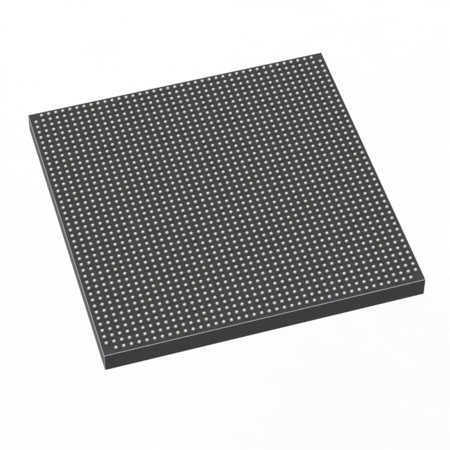
Stratix® V GX Field Programmable Gate Array (FPGA) IC 600 53248000 597000 1760-BBGA, FCBGA |
|---|---|
| Quantity | 1,188 Available (as of June 15, 2026) |

| Product Category | Field Programmable Gate Array (FPGA) |
|---|---|
| Manufacturer | Intel |
| Manufacturing Status | Obsolete |
| Manufacturer Standard Lead Time | Contact Us |
| Datasheet |
Specifications & Environmental
| Device Package | 1760-FCBGA (42.5x42.5) | Grade | Commercial | Operating Temperature | 0°C – 85°C | ||
|---|---|---|---|---|---|---|---|
| Package / Case | 1760-BBGA, FCBGA | Number of I/O | 600 | Voltage | 870 mV - 930 mV | ||
| Mounting Method | Surface Mount | RoHS Compliance | RoHS Compliant | REACH Compliance | REACH Unknown | ||
| Moisture Sensitivity Level | 3 (168 Hours) | Number of LABs/CLBs | 225400 | Number of Logic Elements/Cells | 597000 | ||
| Number of Gates | N/A | ECCN | 3A001A2C | HTS Code | 8542.39.0001 | ||
| Qualification | N/A | Total RAM Bits | 53248000 |
Overview of 5SGXMB6R2F43C2N – Stratix® V GX Field Programmable Gate Array (FPGA) IC, 600 I/O, 597,000 logic elements
The 5SGXMB6R2F43C2N is a Stratix V GX family FPGA from Intel, engineered for high-density, programmable digital designs. It combines a large logic fabric, substantial embedded memory, and a high I/O count in a 1760-FCBGA package.
Designed for applications that require extensive logic resources and on-chip RAM, this commercial-grade device operates over a 0 °C to 85 °C range and supports the Stratix V GX device characteristics documented in the device datasheet, including published transceiver speed grades for the series.
Key Features
- Core Logic Density 597,000 logic elements and 225,400 logic array blocks (LABs) provide a large programmable fabric for complex designs.
- Embedded Memory Approximately 53.2 Mbits of on-chip RAM (total RAM bits: 53,248,000) to support deep buffering, large lookup tables, and state storage without relying solely on external memory.
- High I/O Count 600 device I/O pins enable dense peripheral and high-bandwidth interface integration.
- Power and Voltage Core supply range 870 mV to 930 mV (0.87–0.93 V) to match low-voltage system power domains.
- Package 1760-BBGA, FCBGA (supplier device package: 1760-FCBGA, 42.5 × 42.5 mm) for high-pin-count implementations in a single-chip solution.
- Operating Temperature & Grade Commercial grade with an operating temperature range of 0 °C to 85 °C.
- Regulatory RoHS compliant.
Typical Applications
- Communications and Networking — Large logic density and family-level GX transceiver capabilities documented in the Stratix V datasheet make this device suitable for protocol offload, packet processing, and interface bridging.
- Data Center Acceleration — High logic element and embedded memory counts enable custom acceleration engines and compute offload modules.
- High‑Performance Video and Imaging — Extensive on-chip RAM and abundant logic support parallel pipelines, real-time processing, and multi-channel video interfaces.
- Prototyping and Complex SoC Integration — Dense programmable fabric and 600 I/O simplify integration of multiple subsystems for system validation and prototype platforms.
Unique Advantages
- High integration in a single device: 597,000 logic elements and ~53.2 Mbits of embedded memory reduce the need for external components and simplify board-level design.
- Large I/O footprint: 600 I/Os enable direct connection to a wide set of peripherals, transceivers, and daughter-card interfaces.
- Compact high-pin-count package: 1760-FCBGA (42.5 × 42.5 mm) delivers high connectivity in a compact form factor.
- Low-voltage core operation: 0.87–0.93 V supply range aligns with modern power architectures for efficient system integration.
- Commercial grade with environmental compliance: Rated for 0 °C to 85 °C operation and RoHS compliant for mainstream commercial applications.
- Documented family-level electrical and transceiver characteristics: Stratix V device datasheet provides detailed electrical, switching, and transceiver specifications for design planning.
Why Choose 5SGXMB6R2F43C2N?
The 5SGXMB6R2F43C2N positions itself as a high-density Stratix V GX FPGA offering a combination of large logic capacity, substantial embedded memory, and extensive I/O in a single 1760-FCBGA package. It is well suited for commercial designs that demand on-chip resources to minimize external parts and streamline system architecture.
For engineering teams building complex digital subsystems—ranging from networking and acceleration to high-throughput video processing—this device provides a documented hardware foundation and the on-chip resources needed to scale logic, memory, and interfaces within a single programmable device.
Request a quote or submit an inquiry to receive pricing and availability for part number 5SGXMB6R2F43C2N.


Date Founded: 1968
Headquarters: Santa Clara, California, USA
Employees: 130,000+
Revenue: $54.23 Billion
Certifications and Memberships: ISO9001:2015, ISO14001:2015, ISO17025:2017, ISO27001:2022, ISO45001:2018, ISO50001:2018


