
5SGXMB6R2F43C2LN
| Part Description |
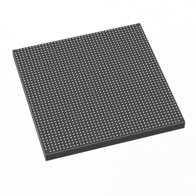
Stratix® V GX Field Programmable Gate Array (FPGA) IC 600 53248000 597000 1760-BBGA, FCBGA |
|---|---|
| Quantity | 1,644 Available (as of June 15, 2026) |
| Product Category | Field Programmable Gate Array (FPGA) |
|---|---|
| Manufacturer | Intel |
| Manufacturing Status | Obsolete |
| Manufacturer Standard Lead Time | Contact Us |
| Datasheet |
Specifications & Environmental
| Device Package | 1760-FCBGA (42.5x42.5) | Grade | Commercial | Operating Temperature | 0°C – 85°C | ||
|---|---|---|---|---|---|---|---|
| Package / Case | 1760-BBGA, FCBGA | Number of I/O | 600 | Voltage | 820 mV - 880 mV | ||
| Mounting Method | Surface Mount | RoHS Compliance | RoHS Compliant | REACH Compliance | REACH Unknown | ||
| Moisture Sensitivity Level | 3 (168 Hours) | Number of LABs/CLBs | 225400 | Number of Logic Elements/Cells | 597000 | ||
| Number of Gates | N/A | ECCN | 3A001A2C | HTS Code | 8542.39.0001 | ||
| Qualification | N/A | Total RAM Bits | 53248000 |
Overview of 5SGXMB6R2F43C2LN – Stratix V GX FPGA, 597,000 logic elements, ~53.25 Mbits RAM, 600 I/Os, 1760-FCBGA
The 5SGXMB6R2F43C2LN is a Stratix® V GX field-programmable gate array (FPGA) IC designed for commercial-grade applications that require substantial programmable logic, embedded memory, and high I/O density. This device integrates 597,000 logic elements and approximately 53.25 Mbits of on-chip RAM to support complex digital designs and high-bandwidth system integration.
With 600 I/Os and a 1760-FCBGA (42.5×42.5 mm) package, the device targets system designs that demand large-scale logic resources, abundant memory, and extensive external connectivity while operating within a commercial temperature range of 0 °C to 85 °C.
Key Features
- High Logic Capacity 597,000 logic elements provide substantial programmable fabric for large, partitioned designs and complex state machines.
- Embedded Memory Approximately 53.25 Mbits of on-chip RAM to support buffering, FIFOs, and large data structures without external memory for many functions.
- Extensive I/O 600 general-purpose I/Os enable wide parallel interfaces, multi-channel connectivity, and dense board-level routing.
- Package and Mounting 1760-FCBGA (42.5×42.5 mm) package in a surface-mount ball-grid array for high-density board integration.
- Power Supply Range Core supply specified from 820 mV to 880 mV to match system power rails and power-management designs.
- Commercial Temperature Grade Rated for operation from 0 °C to 85 °C for commercial applications.
- RoHS Compliant Device meets RoHS requirements for lead-free manufacturing and environmental compliance.
Typical Applications
- High-performance digital processing Use the large logic fabric and embedded RAM for compute-intensive signal processing pipelines and custom accelerators.
- Networking and communications Leverage the high I/O count and on-chip memory for multi-channel packet processing, protocol bridging, and interface aggregation.
- Prototyping and system integration The device’s logic density and I/O capacity make it suitable for consolidating multiple functions onto a single FPGA during prototype and early production phases.
- Embedded compute and control Embedded memory and logic resources support complex control algorithms, state machines, and hardware-software co-designs.
Unique Advantages
- Large programmable fabric: 597,000 logic elements let you implement complex, parallelized logic without partitioning across multiple devices.
- Significant on-chip RAM: Approximately 53.25 Mbits of embedded memory reduces reliance on external DRAM for many buffering and caching needs.
- High I/O density: 600 available I/Os simplify board-level connectivity for multi-channel, multi-protocol systems.
- Commercial-grade operating window: Rated 0 °C to 85 °C for straightforward deployment in commercial environments.
- Compact FCBGA package: 1760-FCBGA (42.5×42.5 mm) enables dense PCB placement while maintaining a high pin count.
- Regulatory readiness: RoHS compliance supports lead-free manufacturing workflows and environmental requirements.
Why Choose 5SGXMB6R2F43C2LN?
The 5SGXMB6R2F43C2LN combines a high logic element count, substantial embedded memory, and a large I/O complement in a single commercial-grade Stratix V GX FPGA package. It is positioned for designs that require consolidation of complex logic, on-chip data storage, and broad external connectivity while operating within typical commercial temperature ranges.
This device is well suited to engineering teams building high-density digital systems, communication modules, and advanced prototypes that benefit from integrated memory and extensive I/O. Its package and electrical specifications support compact board layouts and modern power-rail designs.
To request a quote or submit a parts inquiry for the 5SGXMB6R2F43C2LN, please provide your quantity and delivery requirements and a sales contact will respond with pricing and availability.


Date Founded: 1968
Headquarters: Santa Clara, California, USA
Employees: 130,000+
Revenue: $54.23 Billion
Certifications and Memberships: ISO9001:2015, ISO14001:2015, ISO17025:2017, ISO27001:2022, ISO45001:2018, ISO50001:2018


