
5SGXMB6R2F43C1N
| Part Description |
Stratix® V GX Field Programmable Gate Array (FPGA) IC 600 53248000 597000 1760-BBGA, FCBGA |
|---|---|
| Quantity | 175 Available (as of June 14, 2026) |

| Product Category | Field Programmable Gate Array (FPGA) |
|---|---|
| Manufacturer | Intel |
| Manufacturing Status | Obsolete |
| Manufacturer Standard Lead Time | Contact Us |
| Datasheet |
Specifications & Environmental
| Device Package | 1760-FCBGA (42.5x42.5) | Grade | Commercial | Operating Temperature | 0°C – 85°C | ||
|---|---|---|---|---|---|---|---|
| Package / Case | 1760-BBGA, FCBGA | Number of I/O | 600 | Voltage | 870 mV - 930 mV | ||
| Mounting Method | Surface Mount | RoHS Compliance | RoHS Compliant | REACH Compliance | REACH Unknown | ||
| Moisture Sensitivity Level | 3 (168 Hours) | Number of LABs/CLBs | 225400 | Number of Logic Elements/Cells | 597000 | ||
| Number of Gates | N/A | ECCN | 3A001A2C | HTS Code | 8542.39.0001 | ||
| Qualification | N/A | Total RAM Bits | 53248000 |
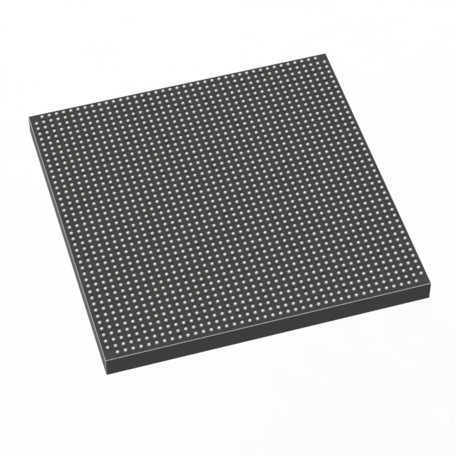
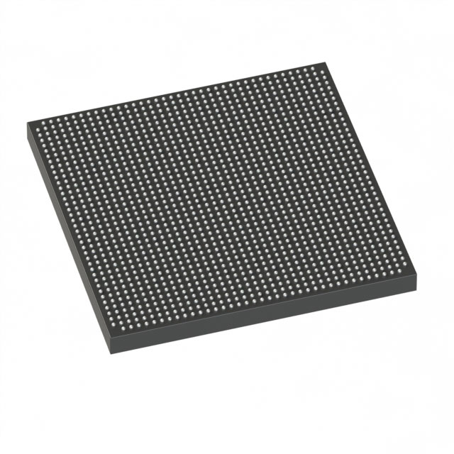
Overview of 5SGXMB6R2F43C1N – Stratix® V GX FPGA (597,000 logic elements, 600 I/O, 1760‑FCBGA)
The 5SGXMB6R2F43C1N is a Stratix® V GX Field Programmable Gate Array (FPGA) from Intel (Altera). It provides high logic density and extensive I/O in a 1760‑ball FCBGA package for demanding commercial designs that require large programmable logic resources and broad connectivity.
With approximately 597,000 logic elements, roughly 53.25 Mbits of embedded memory, and 600 I/O pins, this device targets applications that need substantial on‑chip resources and flexible I/O while operating within commercial temperature and voltage ranges.
Key Features
- Core Logic Approximately 597,000 logic elements to support complex, high‑density logic implementations.
- Embedded Memory Approximately 53.25 Mbits of on‑chip RAM for buffering, lookup tables, and data storage inside the FPGA fabric.
- I/O and Transceiver Support 600 user I/O pins provide extensive external connectivity. As a Stratix V GX device, it is part of the GX family described in the device datasheet for high‑speed I/O and transceiver capabilities.
- Power and Voltage Core supply operating range of 0.87 V to 0.93 V to match system power rails and design constraints.
- Package and Mounting 1760‑FCBGA (42.5 × 42.5 mm) surface‑mount package for dense board integration and reliable mechanical mounting.
- Operating Conditions Commercial grade device rated for 0 °C to 85 °C operating temperature.
- Environmental Compliance RoHS compliant.
Typical Applications
- High‑performance data processing Large logic capacity and substantial embedded RAM enable complex data path acceleration and custom compute pipelines.
- High‑speed communications High I/O count and Stratix V GX family transceiver support suit multi‑lane serial interfaces and packet processing tasks.
- System integration and prototyping Dense programmable fabric and broad connectivity make the device suitable for integration of custom peripherals and system‑level validation.
- Signal processing On‑chip memory and large logic resources support real‑time digital signal processing and filtering implementations.
Unique Advantages
- High logic density: Approximately 597,000 logic elements let you implement large, complex designs on a single device, reducing board count and system complexity.
- Significant embedded memory: Roughly 53.25 Mbits of on‑chip RAM reduces dependence on external memory for many buffering and storage needs.
- Extensive I/O: 600 I/O pins provide flexible interfacing options for multi‑port systems and high channel counts.
- Compact FCBGA package: 1760‑ball FCBGA (42.5 × 42.5 mm) offers high integration density for space‑constrained PCBs.
- Commercial temperature rating: Specified 0 °C to 85 °C operation for standard commercial deployments.
- Regulatory readiness: RoHS compliance addresses common environmental requirements.
Why Choose 5SGXMB6R2F43C1N?
The 5SGXMB6R2F43C1N combines large programmable logic capacity, significant embedded memory, and a very high I/O count in a single commercial‑grade Stratix V GX device from Intel (Altera). These characteristics make it suitable for designs that require consolidation of complex logic, extensive interfacing, and substantial on‑chip storage.
This device is well suited to engineering teams and system designers who need a scalable FPGA platform with strong on‑chip resources and flexible integration options. Its package, voltage range, and datasheet coverage for the Stratix V family support reliable deployment within commercial applications.
Request a quote or submit an inquiry to receive pricing, availability, and technical support for the 5SGXMB6R2F43C1N.


Date Founded: 1968
Headquarters: Santa Clara, California, USA
Employees: 130,000+
Revenue: $54.23 Billion
Certifications and Memberships: ISO9001:2015, ISO14001:2015, ISO17025:2017, ISO27001:2022, ISO45001:2018, ISO50001:2018


