
5SGXMB6R2F40I3LN
| Part Description |
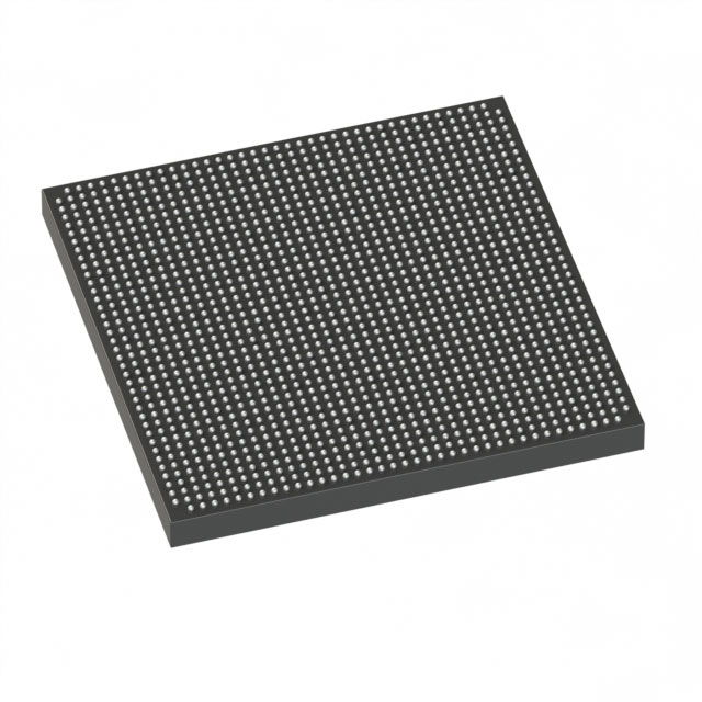
Stratix® V GX Field Programmable Gate Array (FPGA) IC 432 53248000 597000 1517-FBGA (40x40) |
|---|---|
| Quantity | 11 Available (as of June 18, 2026) |

| Product Category | Field Programmable Gate Array (FPGA) |
|---|---|
| Manufacturer | Intel |
| Manufacturing Status | Obsolete |
| Manufacturer Standard Lead Time | Contact Us |
| Datasheet |
Specifications & Environmental
| Device Package | 1517-FBGA (40x40) | Grade | Industrial | Operating Temperature | -40°C – 100°C | ||
|---|---|---|---|---|---|---|---|
| Package / Case | 1517-FBGA (40x40) | Number of I/O | 432 | Voltage | 820 mV - 880 mV | ||
| Mounting Method | Surface Mount | RoHS Compliance | RoHS Compliant | REACH Compliance | REACH Unknown | ||
| Moisture Sensitivity Level | 3 (168 Hours) | Number of LABs/CLBs | 225400 | Number of Logic Elements/Cells | 597000 | ||
| Number of Gates | N/A | ECCN | 3A001A2C | HTS Code | 8542.39.0001 | ||
| Qualification | N/A | Total RAM Bits | 53248000 |
Overview of 5SGXMB6R2F40I3LN – Stratix® V GX Field Programmable Gate Array (FPGA)
The 5SGXMB6R2F40I3LN is a Stratix® V GX field programmable gate array (FPGA) in a 1517-FBGA (40×40) surface-mount package, manufactured by Intel. It delivers a very large logic and memory footprint combined with a high I/O count and industrial temperature operation, making it suitable for designs that require substantial on-chip resources and robust operating range.
As a Stratix V GX family device (series documentation provided), this device aligns with the Stratix V platform characteristics and is intended for applications needing high logic density, extensive embedded RAM, and flexible I/O connectivity within an industrial temperature window.
Key Features
- Logic Capacity — 597,000 logic elements, providing a high-density programmable fabric for complex digital functions and compute-intensive designs.
- Embedded Memory — Approximately 53.25 Mbits of on-chip RAM (53,248,000 bits) to support large buffers, packet queues, and data-path storage without extensive external memory.
- I/O Density — 432 general-purpose I/O pins to enable broad interfacing options to peripherals, sensors, and high-pin-count boards.
- Package & Mounting — 1517-FBGA (40×40) package in a surface-mount form factor for compact board-level integration.
- Voltage Supply — Core supply range of 820 mV to 880 mV, suitable for designs that follow the device’s specified power infrastructure.
- Industrial Temperature Grade — Rated for operation from −40 °C to 100 °C, supporting deployment in environments requiring extended temperature tolerance.
- RoHS Compliant — Meets RoHS environmental requirements for lead-free manufacturing and assembly.
- Stratix V Family Transceiver Information (Series) — Stratix V GX family documentation lists GX channel transceiver speed grades, including channel rates up to 14.1 Gbps (series-level information from device documentation).
Typical Applications
- High-density compute and acceleration — Large logic element and embedded memory capacity support complex algorithms and hardware acceleration blocks inside a single device.
- High-throughput I/O and protocol bridging — High I/O count enables multi-channel interfacing and flexible board-level connectivity for protocol conversion and aggregation.
- Industrial control and ruggedized systems — Industrial temperature rating and robust package make the device suitable for control, imaging, and instrumentation in extended-temperature environments.
Unique Advantages
- High on-chip integration: 597,000 logic elements and approximately 53.25 Mbits of embedded RAM reduce dependence on external logic and memory, simplifying BOM and board complexity.
- Broad interfacing capability: 432 I/Os provide extensive connectivity options for multi-port systems and complex peripheral sets.
- Industrial-grade operation: −40 °C to 100 °C operating range supports deployments in demanding temperature environments.
- Compact, production-ready package: 1517-FBGA (40×40) surface-mount package supports dense PCB layouts and automated assembly flows.
- Documented Stratix V platform: Series documentation includes transceiver and electrical characteristics for Stratix V GX devices, enabling reference to family-level performance and implementation guidance.
Why Choose 5SGXMB6R2F40I3LN?
The 5SGXMB6R2F40I3LN provides a high-capacity Stratix V GX FPGA option for designs demanding substantial logic, large on-chip RAM, and a high number of I/Os within an industrial temperature envelope. Its combination of dense programmable resources and documented Stratix V family characteristics makes it well suited for engineers building compute-intensive, I/O-rich, or ruggedized systems.
Backed by Intel’s Stratix V device documentation, this device offers a clear specification set for power, temperature, and transceiver capabilities at the series level, supporting confident integration into long-life and high-performance designs.
If you would like pricing, availability, or a formal quote for 5SGXMB6R2F40I3LN, request a quote or submit a product inquiry and our team will respond with details.


Date Founded: 1968
Headquarters: Santa Clara, California, USA
Employees: 130,000+
Revenue: $54.23 Billion
Certifications and Memberships: ISO9001:2015, ISO14001:2015, ISO17025:2017, ISO27001:2022, ISO45001:2018, ISO50001:2018


