
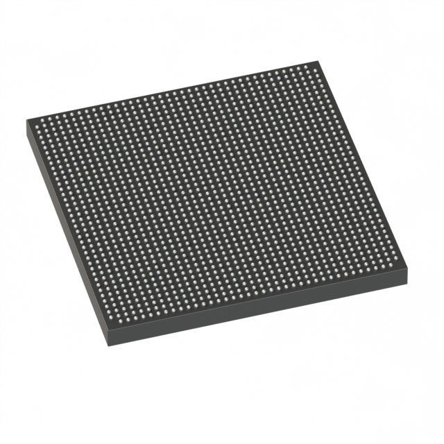
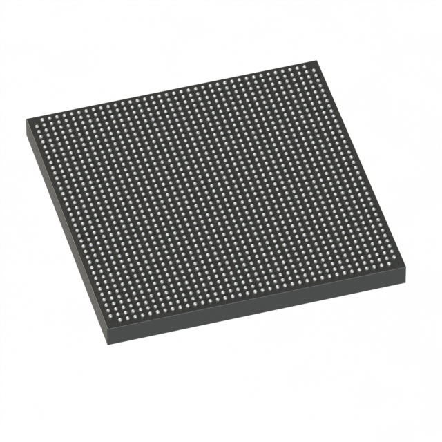
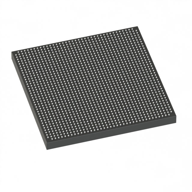
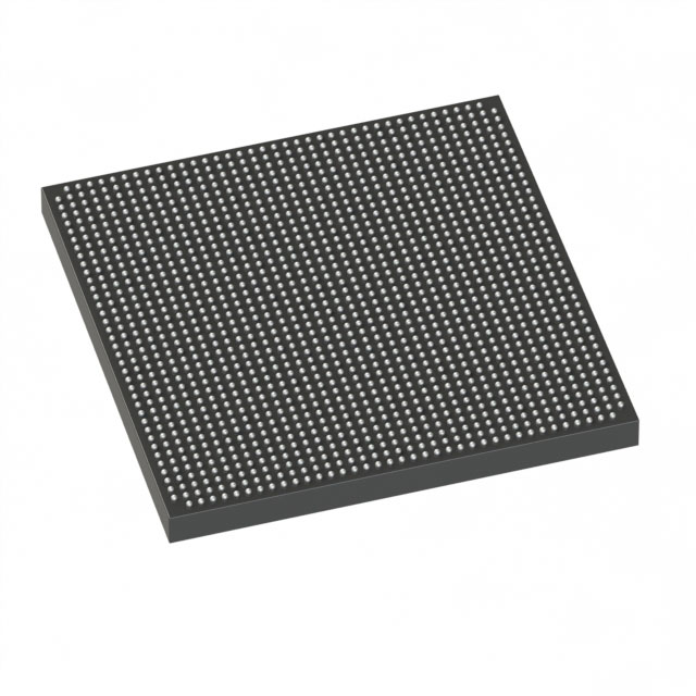
5SGXMB6R2F40I2LN
| Part Description |
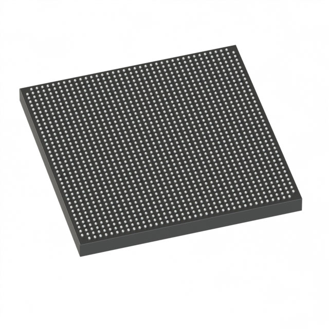
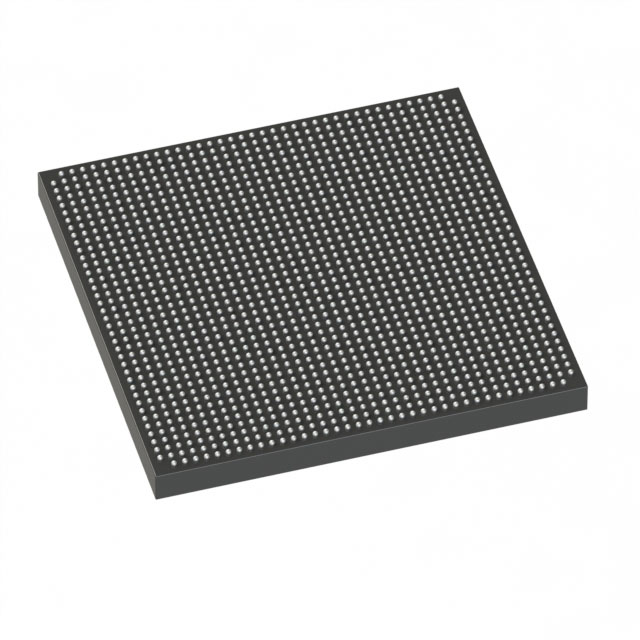
Stratix® V GX Field Programmable Gate Array (FPGA) IC 432 53248000 597000 1517-FBGA (40x40) |
|---|---|
| Quantity | 1,006 Available (as of October 8, 2026) |
| Product Category | Field Programmable Gate Array (FPGA) |
|---|---|
| Manufacturer | Intel |
| Manufacturing Status | Obsolete |
| Manufacturer Standard Lead Time | Contact Us |
| Datasheet |
Specifications & Environmental
| Device Package | 1517-FBGA (40x40) | Grade | Industrial | Operating Temperature | -40°C – 100°C | ||
|---|---|---|---|---|---|---|---|
| Package / Case | 1517-FBGA (40x40) | Number of I/O | 432 | Voltage | 820 mV - 880 mV | ||
| Mounting Method | Surface Mount | RoHS Compliance | RoHS Compliant | REACH Compliance | REACH Unknown | ||
| Moisture Sensitivity Level | 3 (168 Hours) | Number of LABs/CLBs | 225400 | Number of Logic Elements/Cells | 597000 | ||
| Number of Gates | N/A | ECCN | 3A001A2C | HTS Code | 8542.39.0001 | ||
| Qualification | N/A | Total RAM Bits | 53248000 |
Overview of 5SGXMB6R2F40I2LN – Stratix® V GX Field Programmable Gate Array (FPGA)
The 5SGXMB6R2F40I2LN is an Intel Stratix V GX FPGA in a 1517-FBGA (40×40) surface-mount package, offered in an industrial temperature grade. It delivers very large programmable logic and embedded memory resources for complex FPGA designs requiring high I/O counts and robust operating temperature range.
Key on-chip resources include approximately 597,000 logic elements and approximately 53.2 Mbits of total embedded RAM, with 432 user I/Os and a voltage supply window of 820 mV to 880 mV. The Stratix V GX family datasheet also documents transceiver capabilities across multiple speed grades for GX devices.
Key Features
- High logic density — Approximately 597,000 logic elements to implement large-scale digital designs and complex custom logic functions.
- Substantial embedded memory — Approximately 53.2 Mbits of total RAM bits for on-chip buffering, FIFOs, and memory-intensive algorithms.
- Logic block resources — Approximately 225,400 logic blocks (as listed) to structure large designs efficiently.
- General-purpose I/O — 432 I/O pins to support wide parallel interfaces and multiple external peripherals.
- Industrial temperature grade — Rated for operation from −40 °C to 100 °C for deployment in demanding environments.
- Power supply — Core voltage supply range of 820 mV to 880 mV for defined power and performance operating conditions.
- Package and mounting — 1517-FBGA (40×40) supplier device package with surface-mount mounting for board-level integration.
- Environmental compliance — RoHS compliant.
- Stratix V GX family transceiver capability — Datasheet documentation for the Stratix V GX family lists GX channel transceiver speed grades (for the family) up to 14.1 Gbps in certain speed grades.
Unique Advantages
- High on-chip integration: Large logic and memory resources minimize the need for external devices and simplify system BOM for complex FPGA-based systems.
- Robust I/O capacity: 432 I/Os allow flexible interfacing with wide parallel buses, external controllers, and high-pin-count daughter cards.
- Industrial temperature operation: −40 °C to 100 °C rating supports deployment in temperature-challenging applications.
- Defined core voltage window: The 820 mV–880 mV supply range provides a clear operating envelope for power delivery design.
- Surface-mount FBGA package: 1517-FBGA (40×40) enables dense PCB layouts and automated assembly.
- Standards-aligned family documentation: Stratix V GX series datasheet provides detailed electrical and transceiver characteristics to support design and integration.
Why Choose 5SGXMB6R2F40I2LN?
The 5SGXMB6R2F40I2LN brings substantial programmable resources—approximately 597,000 logic elements and roughly 53.2 Mbits of embedded RAM—alongside 432 I/Os in a compact 1517-FBGA (40×40) package. Its industrial temperature grade (−40 °C to 100 °C) and RoHS compliance make it suitable for designs that require durability and regulatory conformance.
Engineers designing high-density, programmable systems will find the device’s defined power envelope and documented Stratix V GX family characteristics useful for power budgeting and high-speed transceiver planning. The combination of integration, I/O capacity, and family-level technical documentation supports scalable, robust FPGA-based solutions.
Request a quote or submit an inquiry to obtain pricing, availability, and further technical information for the 5SGXMB6R2F40I2LN.





















Date Founded: 1968
Headquarters: Santa Clara, California, USA
Employees: 130,000+
Revenue: $54.23 Billion
Certifications and Memberships: ISO9001:2015, ISO14001:2015, ISO17025:2017, ISO27001:2022, ISO45001:2018, ISO50001:2018


