
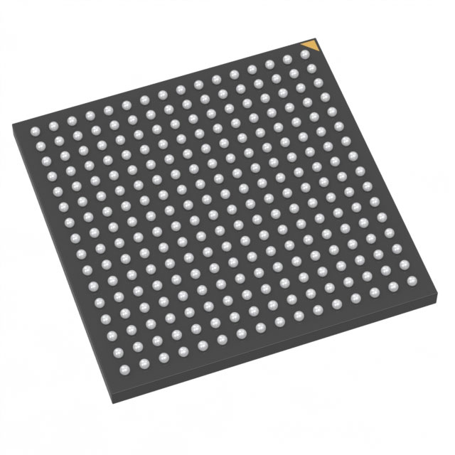
A3P1000L-FGG144
| Part Description |
ProASIC3L Field Programmable Gate Array (FPGA) IC 97 147456 144-LBGA |
|---|---|
| Quantity | 1,502 Available (as of June 15, 2026) |

| Product Category | Field Programmable Gate Array (FPGA) |
|---|---|
| Manufacturer | Microchip Technology |
| Manufacturing Status | Active |
| Manufacturer Standard Lead Time | 8 Weeks |
| Datasheet |
Specifications & Environmental
| Device Package | 144-FPBGA (13x13) | Grade | Commercial | Operating Temperature | 0°C – 85°C | ||
|---|---|---|---|---|---|---|---|
| Package / Case | 144-LBGA | Number of I/O | 97 | Voltage | 1.14 V - 1.575 V | ||
| Mounting Method | Surface Mount | RoHS Compliance | ROHS3 Compliant | REACH Compliance | REACH Unaffected | ||
| Moisture Sensitivity Level | 3 (168 Hours) | Number of LABs/CLBs | 24576 | Number of Logic Elements/Cells | 24576 | ||
| Number of Gates | 1000000 | ECCN | 3A991D | HTS Code | 8542.39.0001 | ||
| Qualification | N/A | Total RAM Bits | 147456 |
Overview of A3P1000L-FGG144 – ProASIC3L FPGA, 1,000,000 gates, 97 I/Os, 144-LBGA
The A3P1000L-FGG144 is a ProASIC3L Field Programmable Gate Array (FPGA) IC designed for commercial electronic designs that require a balance of logic density, on-chip memory, and I/O capability. The device integrates 24,576 logic elements and approximately 0.147 Mbits (147,456 bits) of embedded memory to support medium-complexity digital functions.
With a supply voltage range of 1.14 V to 1.575 V, a 144-LBGA package, and a commercial operating temperature range of 0 °C to 85 °C, this FPGA suits surface-mount board designs where compact packaging and moderate environmental performance are required.
Key Features
- Core Logic 24,576 logic elements providing a total of 1,000,000 gates for implementing custom digital processing, control, and glue-logic functions.
- Embedded Memory Approximately 0.147 Mbits (147,456 bits) of on-chip RAM for buffering, temporary storage, and state retention within user logic.
- I/O Capability 97 available I/Os to support a variety of external interfaces and board-level connectivity requirements.
- Power Operates from a voltage supply of 1.14 V to 1.575 V, enabling compatibility with low-voltage system domains.
- Package & Mounting 144-LBGA package (supplier device package: 144-FPBGA, 13×13) in a surface-mount form factor for compact PCB integration.
- Commercial Grade & Temperature Range Rated for commercial-grade operation from 0 °C to 85 °C to match typical consumer and industrial-adjacent applications.
- Regulatory RoHS compliant, supporting lead-free assembly and regulatory requirements for many commercial products.
Typical Applications
- Embedded Control Systems Implement custom control logic and state machines using available logic elements and on-chip RAM for local buffering.
- I/O Expansion and Glue Logic Leverage 97 I/Os to bridge peripherals, handle bus conversion, and consolidate discrete components into programmable logic.
- Signal Processing and Data Handling Use the FPGA’s logic array and embedded memory for intermediate processing, data alignment, and temporary storage tasks.
- Commercial Electronics Prototyping Support proof-of-concept and production designs where a commercial-grade FPGA with moderate logic density is required.
Unique Advantages
- Balanced Logic Density: 24,576 logic elements and 1,000,000 gates provide sufficient capacity for medium-complexity designs without unnecessary overhead.
- On-chip Memory: Approximately 147,456 bits of embedded RAM reduce the need for external memory in many buffering and state-retention use cases.
- Flexible I/O Count: Ninety-seven I/Os accommodate multiple interfaces and peripheral connections, simplifying board-level integration.
- Compact Surface-Mount Package: 144-LBGA (144-FPBGA, 13×13) footprint enables dense PCB layouts and integration into space-constrained designs.
- Commercial Temperature and RoHS Compliance: Rated for 0 °C to 85 °C operation and RoHS compliant to meet common commercial product and assembly requirements.
- Manufacturer Backing: Produced by Microchip Technology, providing product continuity and access to manufacturer documentation.
Why Choose A3P1000L-FGG144?
The A3P1000L-FGG144 positions itself as a practical FPGA choice for designers who need a mid-range programmable logic device with a clear balance of logic elements, embedded memory, and a substantial I/O count in a compact surface-mount package. Its power and temperature specifications make it suitable for a wide range of commercial electronic designs where on-chip resources and board-level integration are priorities.
This device is well suited to engineering teams developing embedded controllers, interface bridges, and signal-processing blocks that benefit from programmable logic. Backed by Microchip Technology and accompanied by manufacturer documentation, the part offers a straightforward path for designs that require scalability and predictable supply-chain integration.
Request a quote or submit an inquiry to get pricing, availability, and lead-time information for the A3P1000L-FGG144.


Date Founded: 1989
Headquarters: Chandler, Arizona, USA
Employees: 22,000+
Revenue: $8.349 Billion
Certifications and Memberships: ISO9001:2015, IATF16949:2016, AS 9100D


