
EP1AGX50CF484C6N
| Part Description |
Arria GX Field Programmable Gate Array (FPGA) IC 229 2475072 50160 484-BBGA |
|---|---|
| Quantity | 60 Available (as of June 10, 2026) |

| Product Category | Field Programmable Gate Array (FPGA) |
|---|---|
| Manufacturer | Intel |
| Manufacturing Status | Obsolete |
| Manufacturer Standard Lead Time | Contact Us |
| Datasheet |
Specifications & Environmental
| Device Package | 484-FBGA (23x23) | Grade | Commercial | Operating Temperature | 0°C – 85°C | ||
|---|---|---|---|---|---|---|---|
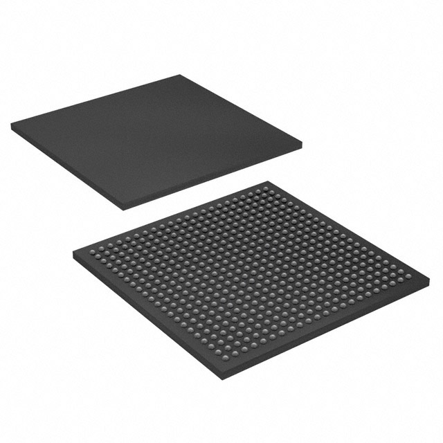
| Package / Case | 484-BBGA | Number of I/O | 229 | Voltage | 1.15 V - 1.25 V | ||
| Mounting Method | Surface Mount | RoHS Compliance | RoHS Compliant | REACH Compliance | REACH Unaffected | ||
| Moisture Sensitivity Level | 3 (168 Hours) | Number of LABs/CLBs | 2508 | Number of Logic Elements/Cells | 50160 | ||
| Number of Gates | N/A | ECCN | 3A001A7A | HTS Code | 8542.39.0001 | ||
| Qualification | N/A | Total RAM Bits | 2475072 |
Overview of EP1AGX50CF484C6N – Arria GX Field Programmable Gate Array (FPGA) IC 229 2475072 50160 484-BBGA
The EP1AGX50CF484C6N is an Intel Arria GX FPGA delivered in a 484-ball BGA package for surface-mount applications. It pairs a 1.2‑V-class logic array architecture with high-density programmable logic and on-chip embedded memory, making it suitable for designs that require substantial logic, I/O capacity, and high-speed serial connectivity.
Typical uses include high-speed communications, video and broadcast interfaces, and DSP-accelerated processing where deterministic I/O count, supply range, and commercial temperature operation are required.
Key Features
- Programmable logic capacity — 50,160 logic elements to implement complex custom logic and control functions.
- On-chip embedded memory — Approximately 2.475 Mbits of total RAM bits, implemented as TriMatrix memory with multiple block sizes for dual-port RAM and FIFO designs.
- I/O and package — 229 user I/O pins in a 484-BBGA (484-FBGA, 23×23) surface-mount package for dense board-level integration.
- High-speed serial capabilities (family-level) — Arria GX family transceivers support up to 3.125 Gbps with CDR and embedded SERDES circuitry for protocol support such as PCI Express, Gigabit Ethernet, SDI, SerialLite II, XAUI, and Serial RapidIO.
- Clocking and timing — Up to 16 global clock networks and up to 32 regional clock networks per device, plus up to four enhanced PLLs for advanced clock management and phase shifting.
- DSP and memory support — Dedicated high-speed DSP blocks for multipliers and MAC operations, and support for high-speed external memory interfaces including DDR and DDR2 (family-level capability).
- Power and operating range — Core supply range from 1.15 V to 1.25 V; commercial operating temperature range of 0 °C to 85 °C.
- Compliance — RoHS-compliant device.
Typical Applications
- High-speed communications — Implement protocol endpoints and bridges for PCI Express, Gigabit Ethernet, and other serial links using the Arria GX transceiver features.
- Broadcast and video transport — SDI and related serial video interfaces benefit from the device’s SERDES and 8B/10B encoding/decoding capabilities.
- Signal processing and DSP — Use dedicated DSP blocks and abundant logic elements for FIR filters, multiply-accumulate tasks, and real-time data processing.
- Memory-interface systems — Act as a controller or bridge for external DDR/DDR2 memory in systems that need on-board buffering and high-throughput data movement.
Unique Advantages
- Substantial logic density: 50,160 logic elements provide headroom for complex FPGA designs without immediate need to migrate to larger devices.
- Integrated, multi-size embedded memory: TriMatrix architecture with approximately 2.475 Mbits of RAM simplifies implementation of FIFOs and dual-port memories.
- Rich I/O and compact packaging: 229 I/O in a 484-ball BGA enables high channel counts in a compact footprint for space-constrained boards.
- High-speed serial-ready (family-level): Transceiver features up to 3.125 Gbps and protocol support help accelerate development of serial-link designs.
- Flexible clocking and DSP resources: Multiple global/regional clock networks, enhanced PLLs, and dedicated DSP blocks streamline timing and compute-intensive tasks.
- Commercial-temperature, RoHS-compliant: Designed for standard commercial applications with environmental compliance for modern assemblies.
Why Choose EP1AGX50CF484C6N?
The EP1AGX50CF484C6N positions itself as a balanced, commercially graded Arria GX FPGA that combines a large programmable logic fabric with substantial embedded memory and a high I/O count in a 484-BBGA footprint. Its supply voltage range and temperature rating make it suitable for mainstream electronic products that need high-density logic and robust timing resources.
This device is well suited to engineering teams building high-speed communications, video transport, and DSP-accelerated systems who require a proven FPGA architecture with integrated clocking, SERDES-capable transceivers (family-level), and dedicated DSP resources to accelerate time-to-market.
If you would like pricing, availability, or a formal quote for EP1AGX50CF484C6N, request a quote or submit a product inquiry and our team will respond with the next steps.


Date Founded: 1968
Headquarters: Santa Clara, California, USA
Employees: 130,000+
Revenue: $54.23 Billion
Certifications and Memberships: ISO9001:2015, ISO14001:2015, ISO17025:2017, ISO27001:2022, ISO45001:2018, ISO50001:2018


