
EP1AGX50CF484I6N
| Part Description |
Arria GX Field Programmable Gate Array (FPGA) IC 229 2475072 50160 484-BBGA |
|---|---|
| Quantity | 925 Available (as of October 7, 2026) |

| Product Category | Field Programmable Gate Array (FPGA) |
|---|---|
| Manufacturer | Intel |
| Manufacturing Status | Obsolete |
| Manufacturer Standard Lead Time | Contact Us |
| Datasheet |
Specifications & Environmental
| Device Package | 484-FBGA (23x23) | Grade | Industrial | Operating Temperature | -40°C – 100°C | ||
|---|---|---|---|---|---|---|---|
| Package / Case | 484-BBGA | Number of I/O | 229 | Voltage | 1.15 V - 1.25 V | ||
| Mounting Method | Surface Mount | RoHS Compliance | RoHS Compliant | REACH Compliance | REACH Unaffected | ||
| Moisture Sensitivity Level | 3 (168 Hours) | Number of LABs/CLBs | 2508 | Number of Logic Elements/Cells | 50160 | ||
| Number of Gates | N/A | ECCN | 3A001A7A | HTS Code | 8542.39.0001 | ||
| Qualification | N/A | Total RAM Bits | 2475072 |
Overview of EP1AGX50CF484I6N – Arria GX FPGA, 50K Logic Elements, 484-BBGA
The EP1AGX50CF484I6N is an Intel Arria GX field-programmable gate array (FPGA) in a 484-ball BGA package designed for industrial applications. It integrates a high-density logic array and embedded memory with the Arria GX family’s high-speed serial transceiver architecture to address mid-to-high complexity system designs.
This device is suited to applications requiring substantial on-chip logic, multi-megabit embedded RAM, broad I/O counts, and operation across an industrial temperature range, while supporting low-voltage core operation for modern system power domains.
Key Features
- Logic Capacity — 50,160 logic elements to implement complex custom logic, control functions, and IP cores.
- Embedded Memory — Approximately 2.48 Mbits of on-chip RAM for implementing FIFOs, buffers and dual-port memory structures.
- I/O Density — 229 user I/O pins to support wide parallel interfaces and mixed-signal board-level connectivity.
- High-speed Serial Transceivers (family) — Arria GX family transceivers support clock-data-recovery and signaling up to 3.125 Gbps; family devices are available with 4, 8, or 12 full-duplex high-speed channels.
- Clocking and DSP (family) — Family-level features include up to 16 global and 32 regional clock networks, high-speed DSP blocks for multiply/accumulate functions, and up to four enhanced PLLs for flexible clock management.
- Memory and External Interfaces (family) — TriMatrix RAM architecture (three RAM block sizes) and support for high-speed external memories such as DDR/DDR2 and SDR SDRAM.
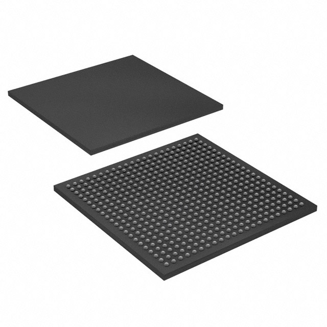
- Package and Mounting — 484-BBGA package; supplier device package listed as 484-FBGA (23×23). Surface-mount device for standard PCB assembly.
- Power — Core voltage supply range: 1.15 V to 1.25 V to match modern low-voltage system rails.
- Industrial Temperature — Rated for operation from −40 °C to 100 °C for deployment in industrial environments.
- Compliance — RoHS compliant.
Typical Applications
- High-speed data interfaces — Implement protocol bridging and SERDES-based links using the Arria GX family transceiver capabilities.
- Embedded control and signal processing — Use the device’s logic density and embedded RAM for control, packet buffering, and on-chip data path processing.
- Communications and networking equipment — Leverage multi-megabit RAM and abundant I/O for packet buffering, interface aggregation, and custom MAC/PHY logic.
- Industrial automation — Broadband I/O and industrial temperature rating make the device suitable for machine control, sensor aggregation, and protocol conversion tasks.
Unique Advantages
- High integration density: 50,160 logic elements reduce external glue logic and simplify complex designs.
- Significant on-chip RAM: Approximately 2.48 Mbits of embedded memory enables large FIFOs, buffering and local data storage without external SRAM.
- Broad I/O capability: 229 I/O pins provide flexibility for parallel buses, high-speed interfaces, and mixed-signal connectivity.
- Industrial robustness: −40 °C to 100 °C operating range supports demanding industrial deployments.
- Low-voltage core: 1.15 V–1.25 V supply range aligns with contemporary power-optimized system designs.
- Proven family-level transceiver and DSP features: Arria GX family transceivers, TriMatrix memory architecture, DSP blocks and advanced PLLs provide a capable platform for serial protocols and signal processing tasks.
Why Choose EP1AGX50CF484I6N?
The EP1AGX50CF484I6N combines substantial logic capacity, multi-megabit embedded RAM, and a high I/O count in a surface-mount 484-BBGA package, making it well suited for mid-to-high complexity industrial systems that require on-chip processing, buffering and flexible interfacing. Its Arria GX family heritage brings serial-transceiver and clocking architectures designed for modern serial protocols and signal-processing workloads.
This device fits customers who need a scalable FPGA platform with proven family-level transceiver and memory architectures, industrial-temperature operation, and RoHS compliance—delivering a balance of integration, performance, and system-level flexibility.
If you would like pricing, availability, or a formal quote for EP1AGX50CF484I6N, please submit a request or contact sales to receive a custom quote.























Date Founded: 1968
Headquarters: Santa Clara, California, USA
Employees: 130,000+
Revenue: $54.23 Billion
Certifications and Memberships: ISO9001:2015, ISO14001:2015, ISO17025:2017, ISO27001:2022, ISO45001:2018, ISO50001:2018


