
EP1C12F256C6
| Part Description |
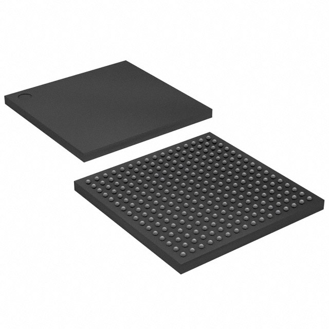
Cyclone® Field Programmable Gate Array (FPGA) IC 185 239616 12060 256-BGA |
|---|---|
| Quantity | 499 Available (as of June 14, 2026) |

| Product Category | Field Programmable Gate Array (FPGA) |
|---|---|
| Manufacturer | Intel |
| Manufacturing Status | Obsolete |
| Manufacturer Standard Lead Time | Contact Us |
| Datasheet |
Specifications & Environmental
| Device Package | 256-FBGA (17x17) | Grade | Commercial | Operating Temperature | 0°C – 85°C | ||
|---|---|---|---|---|---|---|---|
| Package / Case | 256-BGA | Number of I/O | 185 | Voltage | 1.425 V - 1.575 V | ||
| Mounting Method | Surface Mount | RoHS Compliance | RoHS non-compliant | REACH Compliance | REACH Unknown | ||
| Moisture Sensitivity Level | 3 (168 Hours) | Number of LABs/CLBs | 1206 | Number of Logic Elements/Cells | 12060 | ||
| Number of Gates | N/A | ECCN | 3A991D | HTS Code | 8542.39.0001 | ||
| Qualification | N/A | Total RAM Bits | 239616 |
Overview of EP1C12F256C6 – Cyclone® FPGA, 12,060 logic elements, 239,616-bit RAM, 256-BGA
The EP1C12F256C6 is an Intel Cyclone® family SRAM-based field-programmable gate array (FPGA) delivering mid-range logic density and embedded memory for data-path and interface applications. Built on the Cyclone architecture, this device combines approximately 12,060 logic elements with 239,616 bits of on-chip RAM and family-level features aimed at flexible clocking and high-speed I/O.
With 185 user I/O pins in a compact 256-ball FBGA (17×17) package and a core supply range of 1.425 V to 1.575 V, the device is targeted at commercial designs requiring programmable logic, memory resources, and a variety of I/O standards within a surface-mount form factor.
Key Features
- Core Logic Approximately 12,060 logic elements provide mid-range programmable logic capacity for control, data-path, and glue-logic functions.
- Embedded Memory Approximately 0.24 Mbits (239,616 bits) of on-chip RAM, implemented as 52 M4K blocks according to the Cyclone device family data, for FIFOs, buffers, and small on-chip data stores.
- I/O and Interface Support 185 user I/O pins in the 256-FBGA (17×17) package. The Cyclone family supports multiple I/O standards including LVTTL, LVCMOS, SSTL, and LVDS, enabling a range of external interfaces.
- Clocking Two PLLs and family-level clock resources support clock multiplication and phase shifting for synchronous designs and memory interfaces.
- Package & Mounting 256-ball FineLine BGA (256-FBGA, 17×17) package supplied for surface-mount assembly, balancing I/O count and board-area efficiency.
- Power Core supply 1.425 V to 1.575 V, matching the Cyclone family’s 1.5-V process characteristics.
- Operating Conditions & Grade Commercial temperature range, 0 °C to 85 °C.
- Compliance RoHS compliant for environmentally conscious production requirements.
Typical Applications
- Data-Path Processing — Implement custom datapath logic, packet processing, and mid-density compute functions using the device’s logic elements and embedded RAM.
- Memory Interface Controllers — Use integrated clocking and on-chip memory resources to support external memory interfaces such as DDR SDRAM (as supported by Cyclone family features).
- Peripheral and Bus Bridging — Implement PCI-class peripheral bridging and other parallel/serial interfaces leveraging available I/O standards and the device’s I/O count.
- High-Speed I/O and Sensor Interfaces — Deploy LVDS and other supported I/O standards for video, sensor, and high-speed differential signaling applications.
Unique Advantages
- Balanced Logic and Memory: Approximately 12,060 logic elements paired with ~0.24 Mbits of embedded RAM provide a versatile mix for control logic and buffering without external memory for many functions.
- Flexible I/O Options: 185 user I/O pins and family support for multiple I/O standards enable connectivity to a wide range of peripherals and interfaces.
- Integrated Clocking: Two PLLs and dedicated clock resources simplify clock management for synchronous designs and memory interfaces.
- Compact, Surface-Mount Package: 256-FBGA (17×17) provides a high pin-count, space-efficient footprint suitable for compact PCBs.
- Commercial Temperature Range: Rated for 0 °C to 85 °C, suitable for a wide range of commercial embedded applications.
- RoHS Compliant: Conforms to environmental compliance requirements for lead-free assembly.
Why Choose EP1C12F256C6?
The EP1C12F256C6 delivers a practical balance of programmable logic density, embedded memory, and I/O capability within the Cyclone FPGA family architecture. It is well suited for commercial designs that require flexible, reprogrammable logic for data-path tasks, memory interface support, and diverse I/O connectivity while maintaining a compact BGA footprint.
Engineers seeking a mid-density FPGA solution will find this device appropriate for prototypes and production systems that benefit from Cyclone family features such as integrated clocking resources and support for multiple I/O standards, packaged in a RoHS-compliant, surface-mount form factor.
Request a quote or submit an inquiry to receive pricing and availability information for the EP1C12F256C6.


Date Founded: 1968
Headquarters: Santa Clara, California, USA
Employees: 130,000+
Revenue: $54.23 Billion
Certifications and Memberships: ISO9001:2015, ISO14001:2015, ISO17025:2017, ISO27001:2022, ISO45001:2018, ISO50001:2018


