
EP1C12F256C6N
| Part Description |
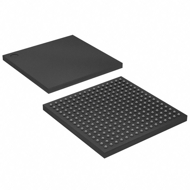
Cyclone® Field Programmable Gate Array (FPGA) IC 185 239616 12060 256-BGA |
|---|---|
| Quantity | 404 Available (as of June 15, 2026) |

| Product Category | Field Programmable Gate Array (FPGA) |
|---|---|
| Manufacturer | Intel |
| Manufacturing Status | Obsolete |
| Manufacturer Standard Lead Time | Contact Us |
| Datasheet |
Specifications & Environmental
| Device Package | 256-FBGA (17x17) | Grade | Commercial | Operating Temperature | 0°C – 85°C | ||
|---|---|---|---|---|---|---|---|
| Package / Case | 256-BGA | Number of I/O | 185 | Voltage | 1.425 V - 1.575 V | ||
| Mounting Method | Surface Mount | RoHS Compliance | Unknown | REACH Compliance | REACH Unknown | ||
| Moisture Sensitivity Level | 3 (168 Hours) | Number of LABs/CLBs | 1206 | Number of Logic Elements/Cells | 12060 | ||
| Number of Gates | N/A | ECCN | 3A991D | HTS Code | 8542.39.0001 | ||
| Qualification | N/A | Total RAM Bits | 239616 |
Overview of EP1C12F256C6N – Cyclone® Field Programmable Gate Array (FPGA) IC 185 239616 12060 256-BGA
The EP1C12F256C6N is a Cyclone® family field programmable gate array (FPGA) from Intel, offering a mid-range integration point with 12,060 logic elements and 239,616 bits of embedded RAM. It implements Cyclone series architectural features and is targeted at data-path and embedded system applications that require flexible logic, on-chip memory, and a moderate I/O count.
Built for commercial-grade applications, this device provides on-chip memory and peripheral interfacing options suitable for memory interfaces, peripheral bridges, and general-purpose programmable logic roles within consumer and commercial electronic products.
Key Features
- Core Density 12,060 logic elements (LEs) providing mid-range programmable logic capacity for combinational and sequential functions.
- Embedded Memory 239,616 total RAM bits (approximately 0.24 Mbits) implemented via 52 M4K RAM blocks for buffering, FIFOs, and small data structures.
- I/O and Interfaces Up to 185 user I/O pins to support peripheral connectivity and board-level interfaces; family-level support includes LVTTL, LVCMOS, SSTL-2, SSTL-3 and LVDS I/O standards as documented for Cyclone devices.
- Clocking Up to two PLLs per device to enable clock multiplication and phase shifting for custom timing domains.
- Power Supply Core voltage supply range 1.425 V to 1.575 V.
- Package & Mounting 256-ball FineLine BGA (256-FBGA, 17 × 17) in a surface-mount form factor for compact board integration.
- Operating Range & Grade Commercial temperature rating with specified operating temperature from 0 °C to 85 °C.
- Environmental Compliance RoHS compliant.
Typical Applications
- Data-path and Memory Interfaces Use the device’s embedded RAM and PLL resources to implement DDR/FCRAM interface logic and buffering for memory subsystems.
- Peripheral Bridges and Protocol Glue Implement custom protocol conversion, bus bridging, or glue logic between ASSP/ASIC components and system peripherals using available I/O and logic resources.
- Embedded Control and Signal Processing Deploy as a programmable controller for embedded systems that require flexible state machines, I/O management, and local data buffering.
- Prototyping and Design Migration Suitable for migrating or prototyping designs within the Cyclone family where vertical device migration is supported by family pinouts and software tools.
Unique Advantages
- Balanced Logic and Memory 12,060 logic elements combined with approximately 0.24 Mbits of embedded memory lets you implement mid-scale logic and local data storage without external RAM for many use cases.
- Moderate I/O Count 185 user I/O pins provide sufficient connectivity for multi-peripheral designs while keeping board routing manageable.
- On-chip Clocking Flexibility Two PLLs enable localized clock domain generation and phase adjustments for timing-critical interfaces.
- Compact BGA Package The 256-FBGA (17 × 17) package supports high-density board designs and surface-mount assembly.
- Commercial Temperature and RoHS Compliance Commercial operating range (0 °C to 85 °C) and RoHS compliance facilitate integration into consumer and commercial product lines.
- Family Resources and Tool Support As a Cyclone family device, it benefits from family-level IP and migration support documented for Cyclone devices, aiding design portability and reuse.
Why Choose EP1C12F256C6N?
The EP1C12F256C6N positions itself as a practical mid-range Cyclone FPGA option where a balance of programmable logic, embedded RAM, and moderate I/O is required. Its combination of 12,060 logic elements, approximately 239,616 bits of on-chip RAM, and two PLLs makes it well-suited for data-path tasks, memory interfacing, and embedded control within commercial products.
Designers looking for a compact, surface-mount BGA solution that aligns with Cyclone family migration paths and available IP can leverage this device to simplify BOM and accelerate prototyping and deployment while maintaining predictable electrical and thermal operating envelopes.
Request a quote or submit a pricing inquiry to evaluate EP1C12F256C6N for your next design and get detailed purchasing information and availability.


Date Founded: 1968
Headquarters: Santa Clara, California, USA
Employees: 130,000+
Revenue: $54.23 Billion
Certifications and Memberships: ISO9001:2015, ISO14001:2015, ISO17025:2017, ISO27001:2022, ISO45001:2018, ISO50001:2018


