
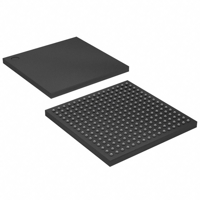
EP1C12F256C6AA
| Part Description |
Cyclone® Field Programmable Gate Array (FPGA) IC 185 239616 12060 256-BGA |
|---|---|
| Quantity | 999 Available (as of June 10, 2026) |

| Product Category | Field Programmable Gate Array (FPGA) |
|---|---|
| Manufacturer | Intel |
| Manufacturing Status | Obsolete |
| Manufacturer Standard Lead Time | Contact Us |
| Datasheet |
Specifications & Environmental
| Device Package | 256-FBGA (17x17) | Grade | Commercial | Operating Temperature | 0°C – 85°C | ||
|---|---|---|---|---|---|---|---|
| Package / Case | 256-BGA | Number of I/O | 185 | Voltage | 1.425 V - 1.575 V | ||
| Mounting Method | Surface Mount | RoHS Compliance | Unknown | REACH Compliance | REACH Unknown | ||
| Moisture Sensitivity Level | 3 (168 Hours) | Number of LABs/CLBs | 1206 | Number of Logic Elements/Cells | 12060 | ||
| Number of Gates | N/A | ECCN | OBSOLETE | HTS Code | 0000.00.0000 | ||
| Qualification | N/A | Total RAM Bits | 239616 |
Overview of EP1C12F256C6AA – Cyclone® Field Programmable Gate Array (FPGA) IC 185 239616 12060 256-BGA
The EP1C12F256C6AA is a Cyclone® family FPGA manufactured by Intel. It is an SRAM-based, reprogrammable logic device implemented on a 1.5‑V, 0.13‑µm all-layer copper process and targeted at moderate-density data-path and control applications.
With 12,060 logic elements, approximately 0.24 Mbits of embedded memory and 185 user I/O pins in a 256‑FBGA (17×17) package, this commercial‑grade, surface‑mount FPGA provides integrated clocking and flexible I/O support for system and interface functions within the 0 °C to 85 °C operating range.
Key Features
- Logic Capacity 12,060 logic elements provide a moderate-density fabric for implementing custom logic, state machines and data-path operations.
- Embedded Memory Approximately 0.24 Mbits of on-chip RAM (239,616 total RAM bits) for buffers, FIFOs and small on-chip data storage.
- I/O Count & Standards 185 user I/O pins with support in the Cyclone family for LVTTL, LVCMOS, SSTL‑2, SSTL‑3 and high‑speed LVDS interfaces, enabling a variety of external connections and signaling standards.
- Clocking Up to two on-chip PLLs (phase-locked loops) per device for clock multiplication and phase shifting to manage multiple clock domains.
- Memory Interfaces Architecture and features in the Cyclone family include support for external memory interfaces such as DDR SDRAM and FCRAM where a dedicated DDR interface is required.
- Package & Mounting 256‑FBGA (17×17) package, surface-mount mounting type, suitable for compact PCB layouts.
- Power & Temperature Device supply range 1.425 V to 1.575 V; commercial operating temperature range 0 °C to 85 °C.
- Regulatory RoHS compliant.
Typical Applications
- Data-path processing Implement custom pipelines, protocol parsing and bit‑level processing using the device’s logic fabric and embedded RAM.
- Memory interface logic Use the device’s DDR interface support and on-chip PLLs to bridge and manage DDR SDRAM or FCRAM in embedded systems.
- High‑speed serial I/O and bridging Leverage LVDS and standard I/O support to implement serial links, interface converters or front-end data acquisition logic.
- Peripheral and subsystem integration Integrate custom control, glue logic or protocol translation between ASSP/ASIC components and system peripherals.
Unique Advantages
- Moderate logic density: 12,060 logic elements let you implement complex control and data-path functions without moving to larger, more costly devices.
- Integrated on‑chip memory: Approximately 0.24 Mbits of embedded RAM reduces external memory dependency for many buffering and local storage needs.
- Flexible I/O and standards support: 185 I/Os plus family support for LVTTL, LVCMOS, SSTL and LVDS provide interface flexibility for mixed-signal systems.
- On‑chip clocking resources: Two PLLs enable clock domain creation and management, simplifying timing architectures across subsystems.
- Compact BGA footprint: 256‑FBGA (17×17) package balances I/O density and PCB area for space-constrained board designs.
- Commercial-grade and RoHS compliant: Designed for 0 °C to 85 °C operation and compliant with RoHS requirements for mainstream industrial and consumer applications.
Why Choose EP1C12F256C6AA?
The EP1C12F256C6AA delivers a balanced combination of logic capacity, embedded memory and flexible I/O in a compact 256‑FBGA package. It is well suited for designers who need moderate-density programmable logic with the ability to implement memory-intense data-paths, multiple I/O standards and integrated clocking without stepping up to higher-density families.
As a member of the Cyclone FPGA family, the device benefits from documented architecture and configuration resources, enabling predictable migration and integration across related Cyclone devices where design scalability and documented migration paths are required.
Request a quote or submit an inquiry to receive pricing and availability information for the EP1C12F256C6AA.


Date Founded: 1968
Headquarters: Santa Clara, California, USA
Employees: 130,000+
Revenue: $54.23 Billion
Certifications and Memberships: ISO9001:2015, ISO14001:2015, ISO17025:2017, ISO27001:2022, ISO45001:2018, ISO50001:2018


