
EP1K10QC208-3N
| Part Description |
ACEX-1K® Field Programmable Gate Array (FPGA) IC 120 12288 576 208-BFQFP |
|---|---|
| Quantity | 102 Available (as of June 15, 2026) |

| Product Category | Field Programmable Gate Array (FPGA) |
|---|---|
| Manufacturer | Intel |
| Manufacturing Status | Obsolete |
| Manufacturer Standard Lead Time | Contact Us |
| Datasheet |
Specifications & Environmental
| Device Package | 208-PQFP (28x28) | Grade | Commercial | Operating Temperature | 0°C – 70°C | ||
|---|---|---|---|---|---|---|---|
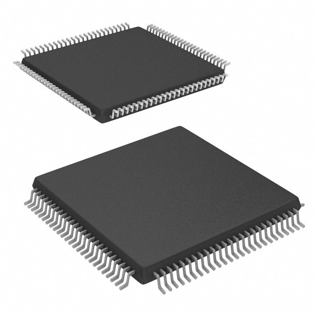
| Package / Case | 208-BFQFP | Number of I/O | 120 | Voltage | 2.375 V - 2.625 V | ||
| Mounting Method | Surface Mount | RoHS Compliance | Unknown | REACH Compliance | REACH Unaffected | ||
| Moisture Sensitivity Level | 3 (168 Hours) | Number of LABs/CLBs | 72 | Number of Logic Elements/Cells | 576 | ||
| Number of Gates | 56000 | ECCN | 3A991D | HTS Code | 8542.39.0001 | ||
| Qualification | N/A | Total RAM Bits | 12288 |
Overview of EP1K10QC208-3N – ACEX-1K FPGA, 120 I/Os, 576 Logic Elements, 208-PQFP
The EP1K10QC208-3N is an ACEX-1K series Field Programmable Gate Array (FPGA) in a 208-pin PQFP package designed for commercial-temperature systems. It combines a programmable logic array with embedded memory blocks to deliver a compact, reconfigurable solution for moderate-density logic, embedded memory functions, and system-level integration.
Typical use cases include custom logic and glue-logic, protocol bridging and communications interfaces, and system-on-a-programmable-chip (SOPC) integration where a balance of I/O count, on-chip RAM, and logic capacity is required.
Key Features
- Core Logic — 576 logic elements providing programmable logic capacity suitable for moderate-density designs; device architecture supports fast arithmetic and cascade functions via dedicated carry and cascade chains.
- Embedded Memory — Total of 12,288 bits of on-chip RAM distributed across embedded array blocks (EABs); dual-port capability and up to 16-bit width per EAB for flexible memory configurations.
- Logic Capacity — Supports up to 56,000 maximum system gates (series data), enabling implementation of larger functions when combined with embedded arrays.
- I/O and Voltage Flexibility — 120 user I/O pins and MultiVolt I/O support that can interface with 2.5 V, 3.3 V, or 5.0 V devices (series feature); individual pin options include programmable slew-rate control and open-drain/clamp options.
- Configuration and Test — In-circuit reconfigurability via external configuration devices and JTAG boundary-scan test (IEEE 1149.1) for board-level test and development.
- Power — Operates with an internal 2.5-V supply; device supply range specified at 2.375 V to 2.625 V to match system power rails.
- Package & Mounting — 208-pin PQFP (28 × 28 mm) surface-mount package (208-BFQFP/PQFP) for conventional PCB assembly and compact board footprint.
- Commercial Temperature & Compliance — Rated for commercial operation from 0 °C to 70 °C and RoHS compliant.
Typical Applications
- Communications Interfaces — Implement protocol conversion, buffering, and timing logic using the combination of logic elements and embedded dual-port RAM.
- System Glue Logic — Replace discrete glue components with a single programmable device to reduce BOM and simplify board routing for mid-volume products.
- Embedded Memory Functions — Use the device’s embedded arrays for small on-chip FIFOs, look-up tables, and packet buffering in data-path designs.
- Custom Control & I/O — 120 programmable I/Os and MultiVolt capability make the device suitable for mixed-voltage interfacing and control functions on commercial systems.
Unique Advantages
- Flexible I/O Interfacing: MultiVolt I/O support and 120 user pins enable direct interfacing to a variety of 2.5 V, 3.3 V, and 5.0 V peripherals without additional level shifters.
- On-chip Dual-Port Memory: 12,288 bits of embedded RAM across EABs simplify the implementation of FIFOs and small data buffers, reducing external memory requirements.
- Reconfigurability and Testability: In-circuit reconfigurability and IEEE 1149.1 JTAG boundary-scan support accelerate development and improve board-level test coverage.
- Compact Surface-Mount Package: 208-pin PQFP (28 × 28 mm) offers a compact footprint for space-constrained PCBs while supporting standard surface-mount assembly processes.
- Commercial-Grade Qualification: Rated for 0 °C to 70 °C operation and RoHS compliant, suitable for mainstream commercial applications.
Why Choose EP1K10QC208-3N?
The EP1K10QC208-3N positions itself as a practical, mid-density FPGA choice for designers who need a blend of programmable logic, embedded RAM, and flexible I/O in a compact PQFP package. Its 576 logic elements, 12,288 bits of on-chip RAM, and support for multi-voltage I/O make it well suited to system glue logic, embedded buffering, and communications interface tasks in commercial systems.
With in-circuit reconfigurability, JTAG boundary-scan support, and a defined supply and temperature envelope, this device offers predictable integration into existing commercial designs and provides a clear upgrade path within the ACEX-1K family.
Request a quote or submit a product inquiry to receive pricing, availability, and ordering assistance for EP1K10QC208-3N.


Date Founded: 1968
Headquarters: Santa Clara, California, USA
Employees: 130,000+
Revenue: $54.23 Billion
Certifications and Memberships: ISO9001:2015, ISO14001:2015, ISO17025:2017, ISO27001:2022, ISO45001:2018, ISO50001:2018


