
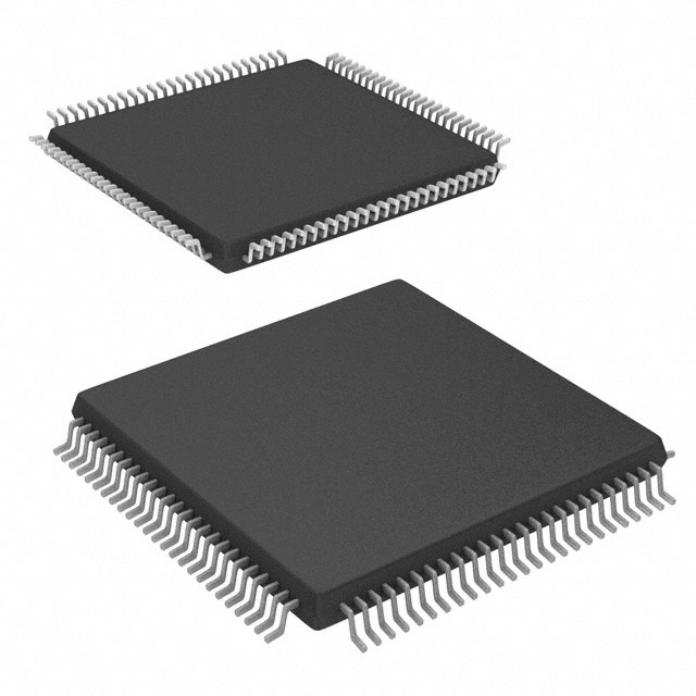
EP1K10TC100-2
| Part Description |
ACEX-1K® Field Programmable Gate Array (FPGA) IC 66 12288 576 100-TQFP |
|---|---|
| Quantity | 123 Available (as of June 15, 2026) |

| Product Category | Field Programmable Gate Array (FPGA) |
|---|---|
| Manufacturer | Intel |
| Manufacturing Status | Obsolete |
| Manufacturer Standard Lead Time | Contact Us |
| Datasheet |
Specifications & Environmental
| Device Package | 100-TQFP (14x14) | Grade | Commercial | Operating Temperature | 0°C – 70°C | ||
|---|---|---|---|---|---|---|---|
| Package / Case | 100-TQFP | Number of I/O | 66 | Voltage | 2.375 V - 2.625 V | ||
| Mounting Method | Surface Mount | RoHS Compliance | RoHS non-compliant | REACH Compliance | REACH Unaffected | ||
| Moisture Sensitivity Level | 3 (168 Hours) | Number of LABs/CLBs | 72 | Number of Logic Elements/Cells | 576 | ||
| Number of Gates | 56000 | ECCN | 3A991D | HTS Code | 8542.39.0001 | ||
| Qualification | N/A | Total RAM Bits | 12288 |
Overview of EP1K10TC100-2 – ACEX-1K® Field Programmable Gate Array (FPGA) IC 66 12288 576 100-TQFP
The EP1K10TC100-2 is an ACEX-1K series programmable logic device from Intel. It combines a logic array and embedded memory blocks to enable system-on-a-programmable-chip (SOPC) integration for compact, reconfigurable designs.
With 576 logic elements, approximately 12,288 bits of on-chip RAM and 66 user I/O pins in a 100-TQFP (14×14) surface-mount package, this commercial-grade device targets communications, embedded control and moderate-density programmable logic applications where integration, in-system reconfigurability and predictable I/O behavior are important.
Key Features
- Logic and density — 576 logic elements and a listed gate count of 56,000 provide moderate programmable logic capacity for control, glue-logic and custom datapath functions.
- Embedded memory — Approximately 12,288 bits of on-chip RAM implemented across the ACEX-1K embedded array blocks (EABs), supporting dual-port operation and up to 16-bit width per block for efficient megafunction implementation.
- I/O and interfacing — 66 user I/O pins; the ACEX-1K family provides MultiVolt I/O capability to interface with 2.5 V, 3.3 V or 5.0 V devices, enabling flexible board-level integration.
- Power and supply — Device operates with a 2.5 V internal supply; listed external supply range 2.375 V to 2.625 V to support the device core voltage requirements.
- Packaging and mounting — 100-TQFP (14×14) surface-mount package for standard PCB assembly and compact board footprint.
- System features and configurability — In-circuit reconfigurability (ICR) via external configuration devices or JTAG, built-in JTAG boundary-scan test circuitry (IEEE 1149.1), and clock management options such as ClockLock and ClockBoost for reduced clock delay and skew.
- Dedicated arithmetic and routing — Dedicated carry and cascade chains plus FastTrack interconnect improve performance and predictability for adders, counters and high-fan-in logic functions.
- Commercial temperature and compliance — Commercial operating temperature range 0 °C to 70 °C and RoHS-compliant construction.
Typical Applications
- Communications modules — Implements protocol glue logic, packet buffering and custom packet-processing functions where embedded RAM and reconfigurable logic reduce BOM and speed time-to-market.
- Embedded control — Provides glue logic, state machines and peripheral interfacing for industrial and consumer embedded controllers that require moderate logic density and reprogrammability.
- System-on-a-programmable-chip (SOPC) — Integrates megafunctions such as small memories and specialized logic blocks to consolidate discrete components and simplify board-level design.
- PCI and legacy bus interfaces — ACEX-1K family features include support relevant to PCI Local Bus implementations (per series datasheet), useful for board-level interface logic in bused systems.
Unique Advantages
- Balanced logic and memory — 576 logic elements combined with embedded RAM (12,288 bits) provide a practical mix for designs that need both custom logic and local data storage.
- Flexible I/O interfacing — MultiVolt I/O capability supports interfacing to a range of voltage domains, simplifying mixed-voltage board designs.
- Reconfigurability and testability — In-circuit reconfigurability and built-in JTAG boundary-scan enable field updates and board-level test without consuming user logic.
- Dedicated architecture for common arithmetic — Carry and cascade chains accelerate adders, counters and comparators while reducing routing overhead for arithmetic-heavy functions.
- Compact package option — 100-TQFP (14×14) surface-mount packaging offers a small footprint for space-constrained boards while maintaining accessible I/O counts.
Why Choose EP1K10TC100-2?
The EP1K10TC100-2 delivers a mid-range ACEX-1K FPGA option for designs that require moderate programmable logic, embedded RAM and flexible I/O in a compact 100-TQFP package. Its combination of logic elements, on-chip memory and series-level system features such as in-circuit reconfigurability and JTAG boundary-scan make it suitable for communications, embedded control and SOPC applications that prioritize integration and field update capability.
For teams seeking a commercially graded, RoHS-compliant FPGA with accessible packaging and a known development ecosystem, the EP1K10TC100-2 provides a straightforward, verifiable building block for a range of board-level programmable logic tasks.
Request a quote or submit a pricing inquiry to evaluate the EP1K10TC100-2 for your next design and confirm availability and lead times.


Date Founded: 1968
Headquarters: Santa Clara, California, USA
Employees: 130,000+
Revenue: $54.23 Billion
Certifications and Memberships: ISO9001:2015, ISO14001:2015, ISO17025:2017, ISO27001:2022, ISO45001:2018, ISO50001:2018


