
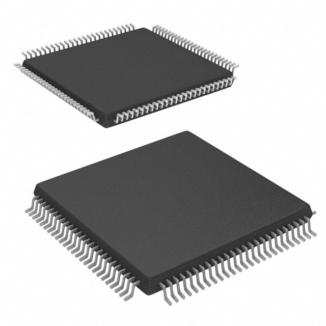
EP1K10TC100-3N
| Part Description |
ACEX-1K® Field Programmable Gate Array (FPGA) IC 66 12288 576 100-TQFP |
|---|---|
| Quantity | 1,399 Available (as of June 14, 2026) |
| Product Category | Field Programmable Gate Array (FPGA) |
|---|---|
| Manufacturer | Intel |
| Manufacturing Status | Obsolete |
| Manufacturer Standard Lead Time | Contact Us |
| Datasheet |
Specifications & Environmental
| Device Package | 100-TQFP (14x14) | Grade | Commercial | Operating Temperature | 0°C – 70°C | ||
|---|---|---|---|---|---|---|---|
| Package / Case | 100-TQFP | Number of I/O | 66 | Voltage | 2.375 V - 2.625 V | ||
| Mounting Method | Surface Mount | RoHS Compliance | Unknown | REACH Compliance | REACH Unaffected | ||
| Moisture Sensitivity Level | 3 (168 Hours) | Number of LABs/CLBs | 72 | Number of Logic Elements/Cells | 576 | ||
| Number of Gates | 56000 | ECCN | 3A991D | HTS Code | 8542.39.0001 | ||
| Qualification | N/A | Total RAM Bits | 12288 |
Overview of EP1K10TC100-3N – ACEX-1K® Field Programmable Gate Array (FPGA) IC 66 12288 576 100-TQFP
The EP1K10TC100-3N is an ACEX-1K family programmable logic device designed for cost-sensitive commercial applications that require flexible, reconfigurable logic and embedded memory. As a member of the ACEX 1K series, it combines a logic array with embedded array blocks (EABs) to enable system-on-a-programmable-chip (SOPC) integration and efficient implementation of memory-intensive megafunctions.
With 576 logic elements, 12,288 total RAM bits, and up to 66 user I/O pins in a 100-TQFP (14×14) surface-mount package, this device targets compact commercial designs where integration, flexible I/O, and in-circuit reconfigurability are important.
Key Features
- Logic Capacity Provides 576 logic elements and a device gate count of 56,000 for implementing combinational and sequential logic functions in compact designs.
- Embedded Memory Total on-chip RAM of 12,288 bits supports data buffering and small embedded memory requirements for megafunctions and dual-port memory usage.
- I/O and Voltage Support Up to 66 user I/O pins with MultiVolt I/O capability in the ACEX 1K family, enabling interaction with a range of peripheral voltage levels. Device internal supply operates at 2.5 V with a supply range of 2.375 V to 2.625 V.
- Package and Mounting Supplied in a 100-TQFP (14×14) surface-mount package suitable for standard PCB assembly processes.
- Commercial Temperature Grade Rated for operation from 0 °C to 70 °C, appropriate for commercial applications and environments.
- In-Circuit Reconfigurability and Test ACEX family devices include JTAG boundary-scan test circuitry and support in-circuit reconfigurability via external configuration devices or the JTAG port.
- Low-Power and Clock Features Family features include low power consumption and built-in clock distribution options (ClockLock and ClockBoost in the series) to support predictable timing in synchronous designs.
- RoHS Compliant Device is RoHS compliant, supporting lead-free assembly requirements.
Typical Applications
- Communications Interfaces Protocol bridging, interface glue logic, and control functions in commercial communications equipment where reconfigurable logic and on-chip memory improve design flexibility.
- SOPC and Embedded Control Integration of custom logic, control state machines, and small embedded functions in system-on-chip style designs to reduce component count.
- Memory Buffering and Data Path Logic Embedded RAM and dual-port array capabilities support buffering, FIFOs, and small memory structures for data flow management.
- General-Purpose Commercial Electronics User interfaces, peripheral control, and custom glue logic in commercial-grade consumer and industrial automation products operating within the specified temperature range.
Unique Advantages
- Compact, reconfigurable logic: 576 logic elements deliver a flexible logic resource for implementing control, glue, and custom functions without adding discrete ASICs or CPLDs.
- Embedded memory for megafunctions: 12,288 bits of on-chip RAM enable efficient implementation of memory-dependent functions and support dual-port memory architectures.
- Flexible I/O voltage handling: MultiVolt family I/O capabilities allow interfacing with a variety of peripheral voltage levels, simplifying mixed-voltage board designs.
- In-circuit reconfigurability and standard test: JTAG boundary-scan and ICR support streamline development, programming, and board-level test flows.
- Standard surface-mount package: 100-TQFP (14×14) packaging supports compact PCB layouts and common assembly processes.
- Regulatory and assembly-friendly: RoHS compliance supports lead-free manufacturing requirements for contemporary production environments.
Why Choose EP1K10TC100-3N?
The EP1K10TC100-3N is positioned for designers who need a commercial-grade, reconfigurable logic device with integrated memory and flexible I/O in a compact 100-TQFP package. Its combination of 576 logic elements, 12,288 bits of embedded RAM, and up to 66 I/O pins provides a balanced resource set for SOPC integration, interface logic, and memory-buffered datapaths.
For teams focused on reducing BOM complexity while preserving design flexibility, this ACEX-1K device offers in-circuit reconfigurability, JTAG test support, and industry-standard packaging—delivering a pragmatic platform for rapid development and production in commercial electronic products.
Request a quote or submit an inquiry to receive pricing, availability, and technical assistance for EP1K10TC100-3N.


Date Founded: 1968
Headquarters: Santa Clara, California, USA
Employees: 130,000+
Revenue: $54.23 Billion
Certifications and Memberships: ISO9001:2015, ISO14001:2015, ISO17025:2017, ISO27001:2022, ISO45001:2018, ISO50001:2018


