
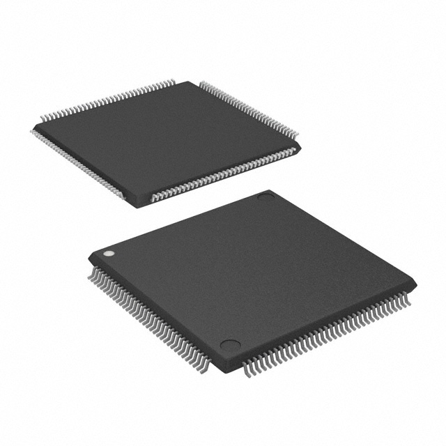
EP1K10TC144-2
| Part Description |
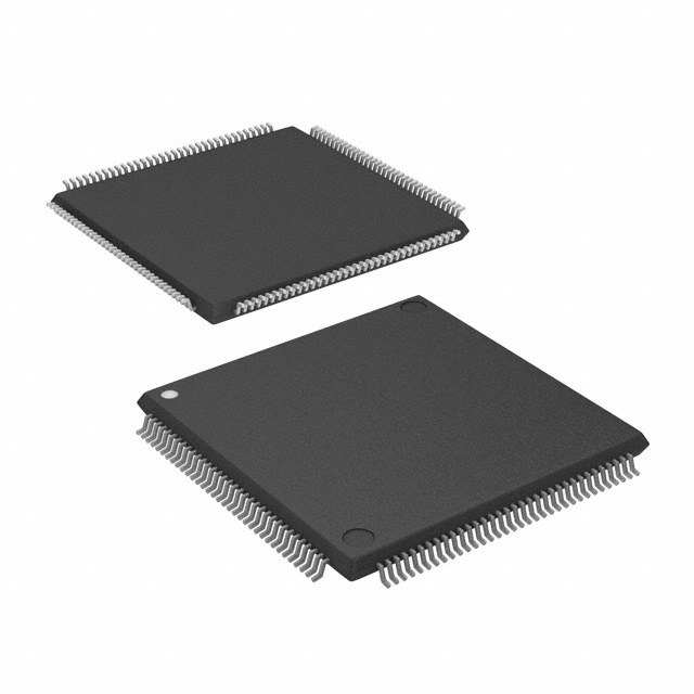
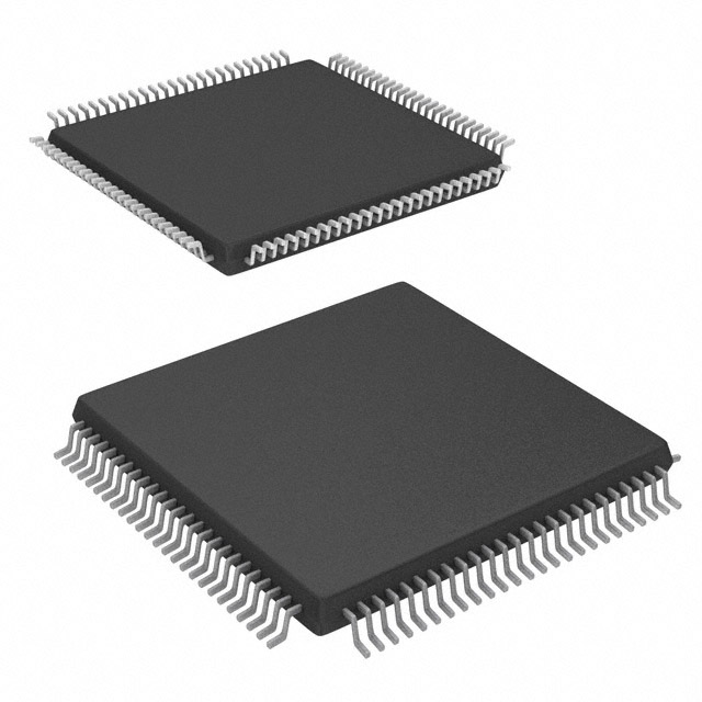
ACEX-1K® Field Programmable Gate Array (FPGA) IC 92 12288 576 144-LQFP |
|---|---|
| Quantity | 314 Available (as of October 8, 2026) |
| Product Category | Field Programmable Gate Array (FPGA) |
|---|---|
| Manufacturer | Intel |
| Manufacturing Status | Obsolete |
| Manufacturer Standard Lead Time | Contact Us |
| Datasheet |
Specifications & Environmental
| Device Package | 144-TQFP (20x20) | Grade | Commercial | Operating Temperature | 0°C – 70°C | ||
|---|---|---|---|---|---|---|---|
| Package / Case | 144-LQFP | Number of I/O | 92 | Voltage | 2.375 V - 2.625 V | ||
| Mounting Method | Surface Mount | RoHS Compliance | RoHS non-compliant | REACH Compliance | REACH Unaffected | ||
| Moisture Sensitivity Level | 3 (168 Hours) | Number of LABs/CLBs | 72 | Number of Logic Elements/Cells | 576 | ||
| Number of Gates | 56000 | ECCN | 3A991D | HTS Code | 8542.39.0001 | ||
| Qualification | N/A | Total RAM Bits | 12288 |
Overview of EP1K10TC144-2 – ACEX-1K® Field Programmable Gate Array (FPGA) IC 92 12288 576 144-LQFP
The EP1K10TC144-2 is a member of the ACEX‑1K programmable logic device family designed for system-on-a-programmable-chip (SOPC) integration. It combines a compact logic fabric with embedded memory blocks and flexible I/O to address mid-density programmable logic requirements in commercial electronic designs.
This device targets applications that require on-chip memory, multiple I/O, and moderate logic capacity while benefitting from cost‑efficient, reconfigurable hardware. It is supplied in a 144‑LQFP surface‑mount package and operates over a commercial temperature range.
Key Features
- Core Logic Approximately 576 logic elements (LEs) providing a mid-density programmable logic resource suitable for SOPC and glue‑logic functions.
- On‑Chip Memory Approximately 12,288 bits of embedded RAM to implement distributed or dual‑port memory structures for buffering, FIFOs, and small data stores.
- I/O Count & Flexibility 92 user I/O pins available for peripheral interfacing and board‑level connectivity in a single 144‑LQFP package.
- Logic Capacity Up to 56,000 system gates for integrating combinational and sequential logic within one device.
- Voltage & Power Operates from a core supply range of 2.375 V to 2.625 V and uses a 2.5‑V internal supply as documented for the ACEX‑1K family.
- Package & Mounting 144‑lead LQFP (surface‑mount) package (supplier device package noted as 144‑TQFP, 20×20), enabling straightforward PCB implementation for production volumes.
- Commercial Temperature Grade Rated for operation from 0 °C to 70 °C, suitable for typical commercial and consumer electronic environments.
- Standards & Testability Series features include JTAG boundary‑scan test circuitry (IEEE 1149.1) to support in‑circuit testing without consuming user logic.
- RoHS Compliant RoHS status: compliant, meeting common lead‑free assembly requirements.
Typical Applications
- Embedded Control & Glue Logic Implement control state machines, protocol translation, and board‑level glue logic where 576 LEs and flexible I/O meet interface and timing needs.
- On‑board Memory Functions Use embedded RAM blocks for small buffers, FIFOs, and dual‑port memory structures in data path or buffering applications.
- Communications & Peripherals Provide protocol handling, I/O aggregation, and peripheral interfacing for communications modules and instrumentation at moderate complexity.
- Prototype and Low‑to‑Medium Volume Products Compact 144‑LQFP package and surface mount mounting make this device practical for production designs and iterative development cycles.
Unique Advantages
- Balanced Logic and Memory The combination of 576 logic elements and ~12,288 bits of embedded RAM lets designers integrate control logic and local data storage on a single device.
- High I/O Density in a Small Package Ninety‑two user I/Os in a 144‑LQFP enable multiple external interfaces while keeping board footprint compact.
- Commercial Ready Designed for commercial temperature operation (0 °C to 70 °C) and RoHS compliance for mainstream electronic products.
- Test and Debug Support Built‑in JTAG boundary‑scan support simplifies manufacturing test and in‑circuit debugging without using user logic resources.
- Cost‑Effective Integration Mid‑density architecture supports integration of multiple functions on one chip, reducing bill of materials and board complexity.
Why Choose EP1K10TC144-2?
The EP1K10TC144-2 delivers a practical balance of logic resources, embedded memory, and I/O count in a compact 144‑LQFP package for commercial applications. Its ACEX‑1K family features—such as embedded RAM blocks and boundary‑scan testability—support system consolidation and streamlined board design.
This device is well suited for design teams who need moderate programmable logic capacity with on‑chip memory and a flexible I/O set within a commercial temperature window, offering straightforward integration into production PCBs and existing tool flows.
Request a quote or submit a request for pricing and availability to begin integrating the EP1K10TC144-2 into your next design.




















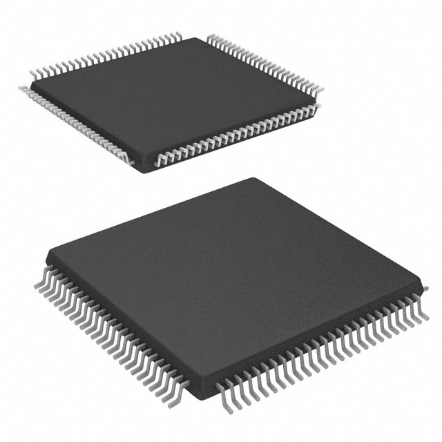
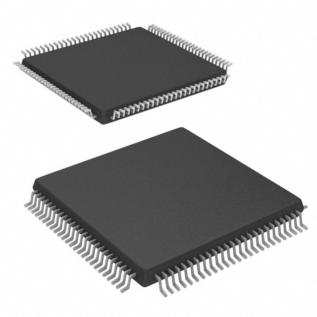
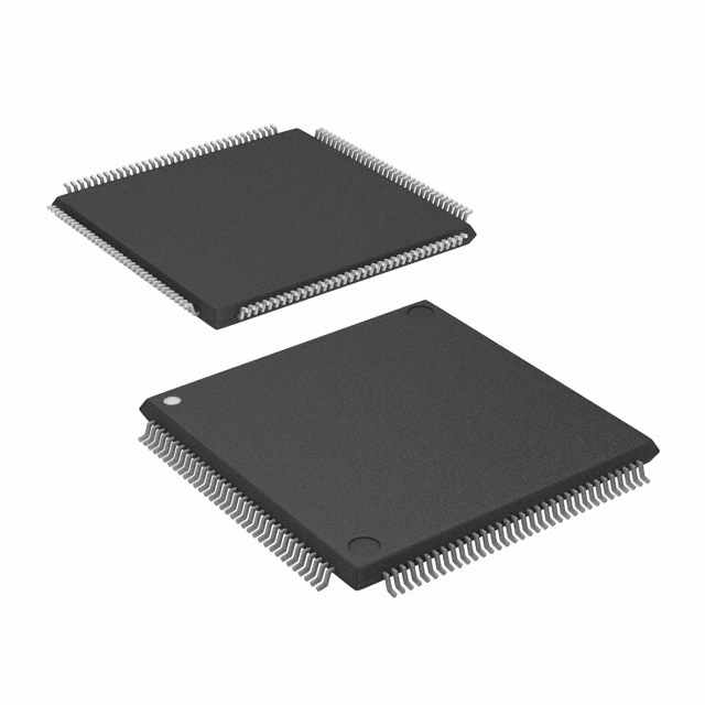

Date Founded: 1968
Headquarters: Santa Clara, California, USA
Employees: 130,000+
Revenue: $54.23 Billion
Certifications and Memberships: ISO9001:2015, ISO14001:2015, ISO17025:2017, ISO27001:2022, ISO45001:2018, ISO50001:2018


