
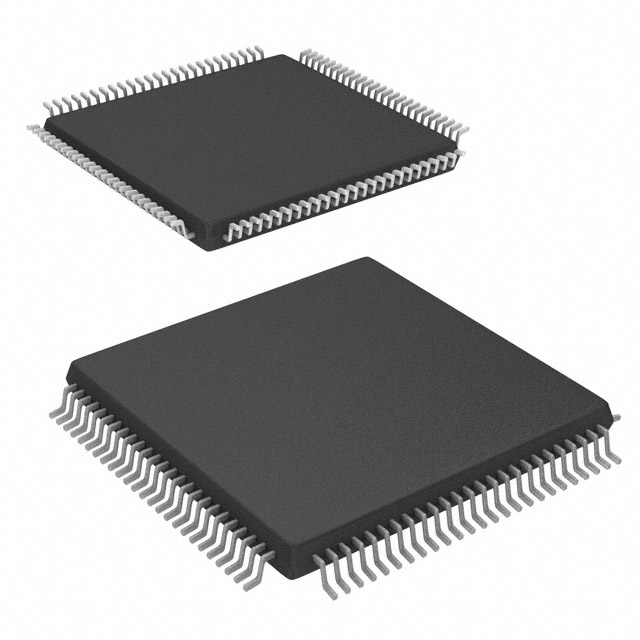
EP1K10TC144-3
| Part Description |
ACEX-1K® Field Programmable Gate Array (FPGA) IC 92 12288 576 144-LQFP |
|---|---|
| Quantity | 815 Available (as of June 17, 2026) |

| Product Category | Field Programmable Gate Array (FPGA) |
|---|---|
| Manufacturer | Intel |
| Manufacturing Status | Obsolete |
| Manufacturer Standard Lead Time | Contact Us |
| Datasheet |
Specifications & Environmental
| Device Package | 144-TQFP (20x20) | Grade | Commercial | Operating Temperature | 0°C – 70°C | ||
|---|---|---|---|---|---|---|---|
| Package / Case | 144-LQFP | Number of I/O | 92 | Voltage | 2.375 V - 2.625 V | ||
| Mounting Method | Surface Mount | RoHS Compliance | RoHS non-compliant | REACH Compliance | REACH Unaffected | ||
| Moisture Sensitivity Level | 3 (168 Hours) | Number of LABs/CLBs | 72 | Number of Logic Elements/Cells | 576 | ||
| Number of Gates | 56000 | ECCN | 3A991D | HTS Code | 8542.39.0001 | ||
| Qualification | N/A | Total RAM Bits | 12288 |
Overview of EP1K10TC144-3 – ACEX-1K® Field Programmable Gate Array (FPGA) IC 92 12288 576 144-LQFP
The EP1K10TC144-3 is a commercial-grade ACEX 1K family FPGA delivering mid-density programmable logic in a 144-LQFP surface-mount package. It integrates 576 logic elements and approximately 12,288 bits of embedded RAM to support system-on-a-programmable-chip (SOPC) integration, efficient memory blocks, and general-purpose logic functions.
Designed for applications such as communications equipment, embedded systems, and custom logic acceleration, this device provides a balance of I/O count (92 pins), on-chip memory, and logic capacity with a 2.375 V to 2.625 V supply range and 0 °C to 70 °C commercial operating temperature.
Key Features
- Logic Capacity 576 logic elements and a gate-equivalent capacity of 56,000 support mid-density logic implementations and combinational/sequential functions.
- Embedded Memory Approximately 12,288 bits of on-chip RAM with embedded-array block (EAB) architecture for efficient implementation of dual-port memories and megafunctions.
- I/O and Voltage 92 user I/O pins with family-level MultiVolt I/O capability to interface with 2.5-V, 3.3-V, or 5.0-V devices; device data lists a supply range of 2.375 V to 2.625 V.
- Package and Mounting 144-LQFP (surface mount) package suitable for compact PCB layouts and standard assembly processes; supplier package listed as 144-TQFP (20×20).
- Configuration and Test Supports in-circuit reconfigurability and includes JTAG boundary-scan (IEEE 1149.1) for board-level test and programming without consuming device logic.
- Clocking and Performance Features Family-level features include built-in low-skew clock distribution, options for reduced clock delay and skew (ClockLock and ClockBoost), and dedicated carry/cascade chains for arithmetic and high-fan-in logic.
- Reliability and Compliance RoHS-compliant lead-free device with commercial-grade operating range (0 °C to 70 °C) and 100% functional testing as part of family qualification.
Typical Applications
- Communications Equipment Use for protocol handling, packet buffering, and interface bridging where mid-range logic density and embedded RAM are required.
- Embedded Systems / SOPC Implement custom peripherals, glue logic, and megafunctions for system-on-a-programmable-chip designs using on-chip RAM and logic array resources.
- Peripheral and Bus Interfaces Integrate bus logic and timing-critical I/O functions; family-level support includes compliance with PCI Local Bus specification for 3.3-V operation (33 MHz/66 MHz).
- Control and Custom Logic Ideal for motor control, sensor interfacing, and UI/control logic requiring flexible I/O, dedicated arithmetic chains, and reprogrammability.
Unique Advantages
- Balanced Integration: Combines 576 logic elements with approximately 12,288 bits of embedded RAM to reduce external memory needs and simplify board-level BOM.
- Flexible I/O Interfacing: Family-level MultiVolt I/O support and 92 user I/O pins enable direct interfacing to a wide range of peripherals and voltage domains.
- Design and Test Support: JTAG boundary-scan and in-circuit reconfigurability streamline programming and manufacturing test flows without consuming logic resources.
- Clocking and Performance Options: Built-in clock distribution, ClockLock/ClockBoost options, and dedicated carry/cascade chains help implement timing-critical functions and arithmetic operations efficiently.
- Proven Family Ecosystem: Part of the ACEX 1K family with documented tools and design flows for synthesis, place-and-route, and megafunction support to accelerate development.
- Compact, Surface-Mount Package: 144-LQFP surface-mount packaging supports space-constrained designs while providing ample I/O for mid-density applications.
Why Choose EP1K10TC144-3?
The EP1K10TC144-3 offers a pragmatic balance of logic, embedded memory, and I/O in a commercial-grade FPGA package. It is well suited for designers who need mid-density programmable logic with on-chip RAM for embedded functions, communications interfaces, and custom control logic while maintaining a compact PCB footprint.
As part of the ACEX 1K family, this device benefits from family-level architectural features—dedicated arithmetic resources, configurable I/O options, and development tool support—making it a reliable choice for projects that require a cost-efficient, reprogrammable logic solution with established design flows.
Request a quote or submit an inquiry to receive pricing and availability for the EP1K10TC144-3 and to discuss how it fits your next design.


Date Founded: 1968
Headquarters: Santa Clara, California, USA
Employees: 130,000+
Revenue: $54.23 Billion
Certifications and Memberships: ISO9001:2015, ISO14001:2015, ISO17025:2017, ISO27001:2022, ISO45001:2018, ISO50001:2018


