
EP1K10TI100-2N
| Part Description |
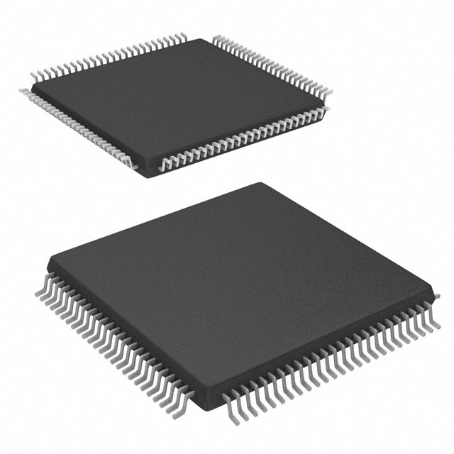
ACEX-1K® Field Programmable Gate Array (FPGA) IC 66 12288 576 100-TQFP |
|---|---|
| Quantity | 557 Available (as of June 14, 2026) |

| Product Category | Field Programmable Gate Array (FPGA) |
|---|---|
| Manufacturer | Intel |
| Manufacturing Status | Obsolete |
| Manufacturer Standard Lead Time | Contact Us |
| Datasheet |
Specifications & Environmental
| Device Package | 100-TQFP (14x14) | Grade | Industrial | Operating Temperature | -40°C – 85°C | ||
|---|---|---|---|---|---|---|---|
| Package / Case | 100-TQFP | Number of I/O | 66 | Voltage | 2.375 V - 2.625 V | ||
| Mounting Method | Surface Mount | RoHS Compliance | Unknown | REACH Compliance | REACH Unaffected | ||
| Moisture Sensitivity Level | 3 (168 Hours) | Number of LABs/CLBs | 72 | Number of Logic Elements/Cells | 576 | ||
| Number of Gates | 56000 | ECCN | 3A991D | HTS Code | 8542.39.0001 | ||
| Qualification | N/A | Total RAM Bits | 12288 |
Overview of EP1K10TI100-2N – ACEX-1K Field Programmable Gate Array (FPGA) IC, 66 I/O, 12,288‑bit RAM, 576 Logic Elements, 100‑TQFP
The EP1K10TI100-2N is an ACEX-1K family field programmable gate array (FPGA) device from Intel, delivering mid-density programmable logic and embedded memory in a compact 100‑TQFP package. It combines on-chip embedded array memory and general logic fabric to implement system-on-programmable-chip (SOPC) functions such as memory macros, specialized logic, and glue logic for industrial designs.
Designed for industrial-grade applications, the device offers 576 logic elements, approximately 12,288 bits of embedded RAM, and 66 user I/O pins, with a specified operating range of −40 °C to 85 °C and a 2.375 V to 2.625 V supply window for the internal core.
Key Features
- Core Logic 576 logic elements provide configurable combinational and sequential resources for implementing custom logic and state machines.
- Embedded Memory Approximately 12,288 bits of on-chip RAM supporting dual-port configurations for efficient buffering and small data-storage functions.
- I/O Capability 66 user I/O pins with multi-volt I/O architecture in the ACEX-1K family—support for interfacing a range of external voltage domains is a defined family feature.
- Performance Density Device silicon supports up to 56,000 system gates (product data lists 56,000 gates), enabling mid-range logic integration within a compact package.
- Package and Mounting 100‑TQFP (14×14) surface-mount package simplifies PCB routing while keeping a small board footprint.
- Industrial Temperature Grade Qualified for operation from −40 °C to 85 °C for deployment in industrial environments.
- Power and Supply Core supply specified at 2.375 V to 2.625 V; device operates with a 2.5‑V internal supply as part of the ACEX-1K family architecture.
- Design & Test Features Family-level features include IEEE 1149.1 JTAG boundary-scan support and in-circuit reconfigurability (ICR) options, enabling board-level test and runtime reconfiguration.
- Clock and Interconnect ACEX-1K family includes built-in low-skew clock distribution and dedicated carry/cascade chains for efficient arithmetic and high-fan-in logic implementations.
- RoHS Compliant Device is RoHS compliant for environmentally conscious designs.
Typical Applications
- Industrial Control Implement control logic, protocol translation, and glue logic in factory automation and process-control modules operating in industrial temperature ranges.
- Communications Equipment Use embedded RAM and dual-port memory capabilities for buffering, packet processing, and interface bridging in mid-density communications designs.
- Embedded Systems Integrate peripheral control, custom interfaces, and small-scale SOPC functions where compact package and reconfigurability are required.
- Prototyping and Low-to-Mid Density FPGA Designs Rapidly validate logic functions and custom IP using the device’s logic elements, embedded memory, and supported design toolflows referenced for the ACEX-1K family.
Unique Advantages
- Compact, Mid‑Density Integration: 576 logic elements with embedded RAM deliver the right balance of logic and memory for compact system designs without excess board-level components.
- Industrial Operating Range: Specified −40 °C to 85 °C operation enables deployment in industrial environments where temperature resilience matters.
- Flexible I/O and Interfacing: Family-level multi-volt I/O support and 66 user I/O pins allow straightforward interfacing to varied external logic levels and peripherals.
- Testability and In‑Circuit Reconfiguration: Built-in JTAG boundary-scan and in-circuit reconfigurability options simplify board bring-up, manufacturing test, and field updates.
- Small Footprint Package: 100‑TQFP (14×14) surface-mount package minimizes PCB area while keeping routing manageable for density-constrained designs.
- Standards‑Oriented Design Flow: ACEX-1K family design support includes common EDA interfaces and tools, facilitating integration into existing development flows.
Why Choose EP1K10TI100-2N?
The EP1K10TI100-2N positions itself as a practical mid-density FPGA choice for industrial and embedded applications that require on-chip RAM, flexible I/O, and reconfigurable logic in a compact 100‑TQFP package. Its combination of 576 logic elements and approximately 12,288 bits of embedded memory supports system-on-programmable-chip use cases such as interface bridging, buffering, and control logic integration.
Backed by the ACEX-1K family feature set—including JTAG boundary-scan, in-circuit reconfigurability, dedicated arithmetic chains, and family-level tool support—this device is suitable for engineers seeking a balanced, industrial-grade FPGA solution with clear, verifiable specifications for production and fielded systems.
Request a quote or submit a procurement inquiry to evaluate EP1K10TI100-2N for your next industrial or embedded FPGA design project.


Date Founded: 1968
Headquarters: Santa Clara, California, USA
Employees: 130,000+
Revenue: $54.23 Billion
Certifications and Memberships: ISO9001:2015, ISO14001:2015, ISO17025:2017, ISO27001:2022, ISO45001:2018, ISO50001:2018


