
EP1K10TC100-1N
| Part Description |
ACEX-1K® Field Programmable Gate Array (FPGA) IC 66 12288 576 100-TQFP |
|---|---|
| Quantity | 355 Available (as of June 15, 2026) |

| Product Category | Field Programmable Gate Array (FPGA) |
|---|---|
| Manufacturer | Intel |
| Manufacturing Status | Obsolete |
| Manufacturer Standard Lead Time | Contact Us |
| Datasheet |
Specifications & Environmental
| Device Package | 100-TQFP (14x14) | Grade | Commercial | Operating Temperature | 0°C – 70°C | ||
|---|---|---|---|---|---|---|---|
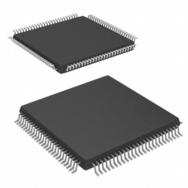
| Package / Case | 100-TQFP | Number of I/O | 66 | Voltage | 2.375 V - 2.625 V | ||
| Mounting Method | Surface Mount | RoHS Compliance | Unknown | REACH Compliance | REACH Unaffected | ||
| Moisture Sensitivity Level | 3 (168 Hours) | Number of LABs/CLBs | 72 | Number of Logic Elements/Cells | 576 | ||
| Number of Gates | 56000 | ECCN | 3A991D | HTS Code | 8542.39.0001 | ||
| Qualification | N/A | Total RAM Bits | 12288 |
Overview of EP1K10TC100-1N – ACEX-1K® Field Programmable Gate Array (FPGA) IC 66 12288 576 100-TQFP
The EP1K10TC100-1N is a member of the ACEX‑1K programmable logic device family, providing a compact FPGA with embedded memory for low-cost system-on-a-programmable-chip (SOPC) integration. It combines 576 logic elements, approximately 56,000 gates, and 12,288 bits of on-chip RAM with a 100‑pin TQFP surface-mount package.
Targeted at commercial applications, this device offers in-circuit reconfigurability, a 2.375 V to 2.625 V supply range (operating with a 2.5 V internal supply), and 66 user I/O pins — making it suited for memory-intensive logic, interface bridging, and embedded control functions within the 0 °C to 70 °C operating range.
Key Features
- Core Logic 576 logic elements and approximately 56,000 gates provide the fabric for custom logic, glue, and control functions.
- Embedded Memory (EABs) Three embedded array blocks (EABs) delivering a total of 12,288 RAM bits; EABs support dual-port operation with up to 16‑bit width per block for efficient on-chip storage and megafunction implementation.
- I/O and Voltage Support 66 user I/O pins with MultiVolt I/O capability (family feature) to interface with a range of device voltages; device operates from a 2.375 V to 2.625 V supply and uses a 2.5 V internal core supply.
- Configuration & Test In-circuit reconfigurability and built-in JTAG boundary-scan test (IEEE 1149.1) enable field updates and board-level test without consuming user logic.
- Clocking & Timing Family-level features include low-skew clock distribution, ClockLock and ClockBoost options for reduced clock delay and skew, and dedicated carry/cascade chains for high-speed arithmetic and logic functions.
- Package & Mounting Surface-mount 100‑TQFP (14 × 14 mm) package for compact board integration and straightforward PCB routing.
- Compliance & Environmental RoHS‑compliant device, commercial grade with an operating temperature range of 0 °C to 70 °C.
Typical Applications
- Communications Interfaces Use embedded arrays and dual-port memory to implement protocol buffering, data alignment, and interface bridging in communications endpoints and edge devices.
- Embedded Control and Glue Logic Leverage the logic elements and I/O count for system glue, peripheral control, and finite-state-machine implementations in compact embedded systems.
- On‑chip Memory Functions Implement small frame buffers, FIFOs, and lookup tables using the 12,288 bits of embedded RAM and dual-port capability for concurrent access patterns.
- Prototyping and Low‑cost Production The 100‑TQFP package and commercial-grade specification make the device suitable for rapid development boards and cost-sensitive production runs.
Unique Advantages
- Highly integrated FPGA Combines logic, embedded RAM, and I/O in a single 100‑TQFP package to reduce BOM and board area.
- On‑chip dual-port memory EABs with dual-port capability simplify designs requiring concurrent read/write access and shared memory between functional blocks.
- Flexible I/O interfacing MultiVolt I/O family features enable interfacing with different voltage domains, easing integration with mixed-voltage peripherals.
- Field reconfigurable In‑circuit reconfigurability and JTAG support streamline post‑assembly updates and in-field fixes without redesigning hardware.
- Compact SMT package 100‑TQFP (14×14) provides a balance of density and accessibility for debug and prototyping while supporting surface-mount assembly.
- Regulatory and environmental alignment RoHS compliance supports environmentally conscious product designs and supply chain requirements.
Why Choose EP1K10TC100-1N?
The EP1K10TC100-1N is positioned for engineers who need a compact, commercially graded FPGA that combines logic capacity, embedded memory, and flexible I/O in a space-efficient 100‑TQFP package. With 576 logic elements, 12,288 bits of on‑chip RAM, and in‑circuit reconfigurability, it supports a wide range of memory‑centric and control applications where board-level integration and reprogrammability matter.
Choose this device when you need predictable, verifiable FPGA capability for commercial-temperature environments, a reduced BOM through on-chip resources, and the ability to update functionality in the field while maintaining RoHS compliance.
Request a quote or submit an inquiry to our sales team to check availability, pricing, and lead-time for EP1K10TC100-1N.


Date Founded: 1968
Headquarters: Santa Clara, California, USA
Employees: 130,000+
Revenue: $54.23 Billion
Certifications and Memberships: ISO9001:2015, ISO14001:2015, ISO17025:2017, ISO27001:2022, ISO45001:2018, ISO50001:2018


