
EP1K10QC208-3
| Part Description |
ACEX-1K® Field Programmable Gate Array (FPGA) IC 120 12288 576 208-BFQFP |
|---|---|
| Quantity | 290 Available (as of June 18, 2026) |

| Product Category | Field Programmable Gate Array (FPGA) |
|---|---|
| Manufacturer | Intel |
| Manufacturing Status | Obsolete |
| Manufacturer Standard Lead Time | Contact Us |
| Datasheet |
Specifications & Environmental
| Device Package | 208-PQFP (28x28) | Grade | Commercial | Operating Temperature | 0°C – 70°C | ||
|---|---|---|---|---|---|---|---|
| Package / Case | 208-BFQFP | Number of I/O | 120 | Voltage | 2.375 V - 2.625 V | ||
| Mounting Method | Surface Mount | RoHS Compliance | RoHS non-compliant | REACH Compliance | REACH Unaffected | ||
| Moisture Sensitivity Level | 3 (168 Hours) | Number of LABs/CLBs | 72 | Number of Logic Elements/Cells | 576 | ||
| Number of Gates | 56000 | ECCN | 3A991D | HTS Code | 8542.39.0001 | ||
| Qualification | N/A | Total RAM Bits | 12288 |
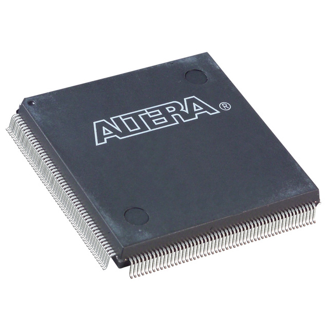
Overview of EP1K10QC208-3 – ACEX-1K FPGA, 576 logic elements, 12,288-bit embedded RAM, 120 I/Os
The EP1K10QC208-3 is an ACEX-1K field programmable gate array (FPGA) from Intel designed for moderate-density, cost-efficient system integration. It combines a logic array with embedded array blocks (EABs) to support megafunctions such as dual-port memory and specialized logic, enabling system-on-a-programmable-chip (SOPC) architectures for communications, embedded control, and peripheral interfacing.
Built for commercial applications, the device provides in-circuit reconfigurability, MultiVolt I/O flexibility, and a 208-pin BFQFP surface-mount package, making it suitable for compact board-level designs that require reprogrammable logic and on-chip memory.
Key Features
- Logic Capacity — 576 logic elements (LEs) and approximately 56,000 gates for medium-density logic integration.
- Embedded Memory — 12,288 total RAM bits implemented across embedded array blocks (EABs) to support dual-port memory and storage of intermediate data and state.
- I/O and Voltage — 120 user I/O pins with MultiVolt I/O capability described by the ACEX-1K family; device uses a 2.5 V internal supply and requires an external voltage supply of 2.375 V to 2.625 V.
- Package & Mounting — Surface-mount 208-BFQFP package (supplier device package: 208-PQFP, 28×28 mm) for compact PCB implementations.
- Reconfigurability & Test — In-circuit reconfigurability via external configuration devices, intelligent controllers, or the JTAG port; built-in JTAG boundary-scan (IEEE Std. 1149.1-1990) for board-level testing.
- Clocking & Timing — Built-in low-skew clock distribution with ClockLock and ClockBoost options, support for up to six global clock signals and four global clear signals to simplify synchronous design.
- Interconnect & Arithmetic Support — FastTrack continuous routing architecture, dedicated carry and cascade chains for efficient implementation of adders, counters, comparators, and high-fan-in logic.
- Operating Range & Grade — Commercial grade with an operating temperature range of 0 °C to 70 °C.
- Standards & Performance — Family-level support for PCI Local Bus operation at 3.3 V (per the ACEX-1K datasheet) and low power consumption characteristics described for the product family.
- RoHS Compliance — Device is RoHS compliant.
Typical Applications
- Communications Equipment — Packet processing, protocol bridging, and custom timing/logic functions that leverage on-chip memory and reconfigurable logic.
- Embedded Systems — SOPC integration where dual-port EABs and dedicated arithmetic chains accelerate storage and control functions on a single device.
- Peripheral Interfaces and PCI-based Designs — Board-level interface logic for systems requiring 3.3 V PCI Local Bus compatibility at standard bus frequencies (as supported at the family level).
- Custom Logic and Glue Logic — Compact, surface-mount FPGA for implementing application-specific control, signal conditioning, or glue logic between subsystems.
Unique Advantages
- Moderate-density integration: 576 logic elements and 12,288 bits of embedded RAM provide a balanced mix of logic and memory for mid-range designs without excessive BOM complexity.
- On-chip dual-port memory: Embedded array blocks support dual-port operation enabling efficient shared-memory architectures and pipeline buffering.
- Flexible I/O and supply: 120 user I/Os combined with a 2.5 V internal supply and MultiVolt I/O capabilities (family-level) simplify board-level interfacing with a range of device voltages.
- Reconfigurability and testability: In-circuit reconfiguration plus integrated JTAG boundary-scan support reduce development and test cycle time for iterative designs and production testing.
- Clock and arithmetic support: Low-skew clock trees, ClockLock/ClockBoost options, and dedicated carry/cascade chains help implement high-performance synchronous logic and arithmetic functions.
- Compact package: 208-pin BFQFP surface-mount package enables integration into space-constrained PCBs while exposing 120 I/Os for system connectivity.
Why Choose EP1K10QC208-3?
The EP1K10QC208-3 delivers a practical combination of reprogrammable logic, embedded memory, and flexible I/O in a compact 208-BFQFP package, making it well suited for commercial embedded and communications designs that need in-field configurability and on-chip storage. Its family-level features—such as JTAG boundary-scan, FastTrack interconnect, dedicated carry/cascade chains, and clock distribution options—support predictable timing and efficient implementation of common logic and memory-intensive functions.
Designers targeting moderate-density FPGA implementations will find this device appropriate for reducing external component count while retaining the ability to iterate and update designs via in-circuit reconfiguration. Development and implementation are supported by the ACEX-1K product family toolset and design flows described in the device documentation.
Request a quote or submit a parts inquiry to begin procurement of the EP1K10QC208-3 for your next project.


Date Founded: 1968
Headquarters: Santa Clara, California, USA
Employees: 130,000+
Revenue: $54.23 Billion
Certifications and Memberships: ISO9001:2015, ISO14001:2015, ISO17025:2017, ISO27001:2022, ISO45001:2018, ISO50001:2018


