
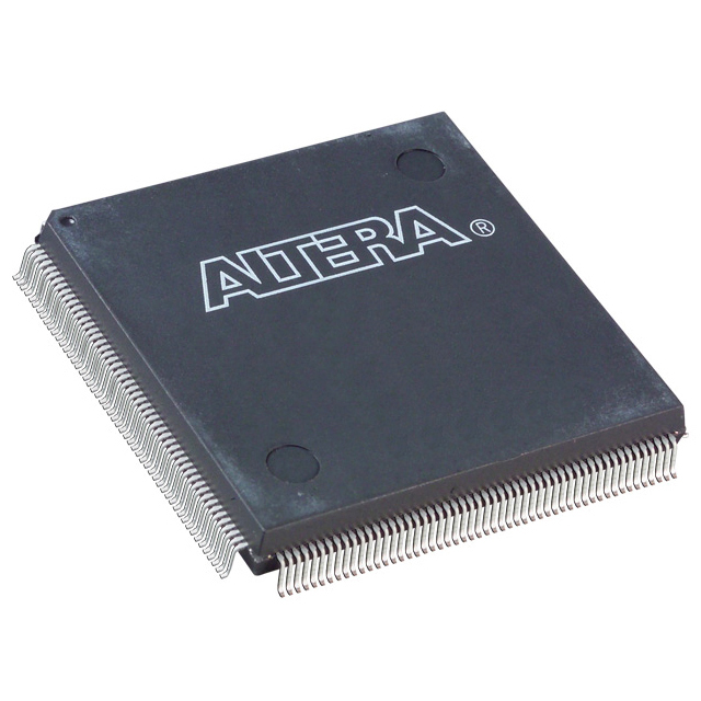
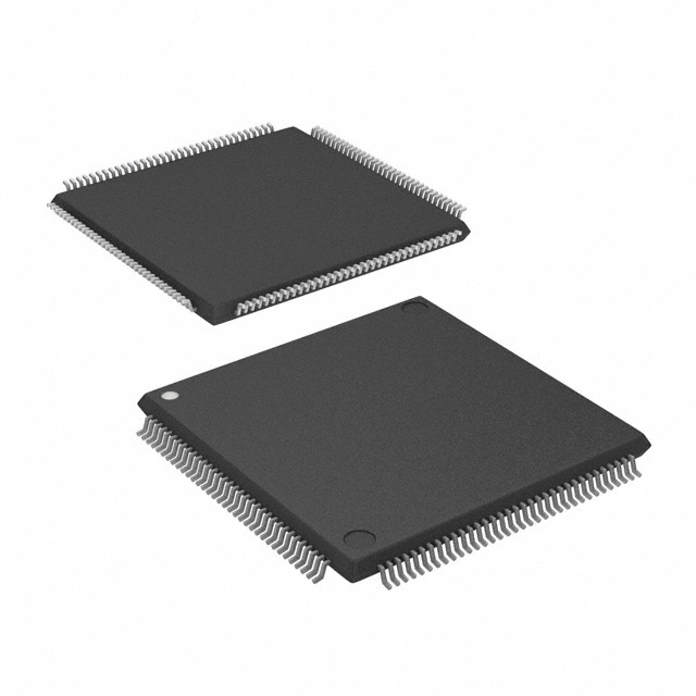
EP1K50TC144-2N
| Part Description |
ACEX-1K® Field Programmable Gate Array (FPGA) IC 102 40960 2880 144-LQFP |
|---|---|
| Quantity | 668 Available (as of June 14, 2026) |

| Product Category | Field Programmable Gate Array (FPGA) |
|---|---|
| Manufacturer | Intel |
| Manufacturing Status | Obsolete |
| Manufacturer Standard Lead Time | Contact Us |
| Datasheet |
Specifications & Environmental
| Device Package | 144-TQFP (20x20) | Grade | Commercial | Operating Temperature | 0°C – 70°C | ||
|---|---|---|---|---|---|---|---|
| Package / Case | 144-LQFP | Number of I/O | 102 | Voltage | 2.375 V - 2.625 V | ||
| Mounting Method | Surface Mount | RoHS Compliance | Unknown | REACH Compliance | REACH Unaffected | ||
| Moisture Sensitivity Level | 3 (168 Hours) | Number of LABs/CLBs | 360 | Number of Logic Elements/Cells | 2880 | ||
| Number of Gates | 199000 | ECCN | 3A991D | HTS Code | 8542.39.0001 | ||
| Qualification | N/A | Total RAM Bits | 40960 |
Overview of EP1K50TC144-2N – ACEX-1K® Field Programmable Gate Array (FPGA) IC 102 40960 2880 144-LQFP
The EP1K50TC144-2N is an ACEX-1K family programmable logic device designed for commercial electronic systems that require moderate logic density with embedded memory. Built on the ACEX-1K architecture, it combines a logic array, embedded array blocks (EABs) and flexible I/O to implement system-on-a-programmable-chip (SOPC) functions and specialized megafunctions.
With 2,880 logic elements, approximately 40,960 bits of embedded RAM, and support for MultiVolt I/O and in-circuit reconfigurability, this device targets applications such as communications interfaces, protocol bridging, and custom logic integration where compact, reprogrammable logic and on-chip memory are required.
Key Features
- Logic Capacity Provides 2,880 logic elements and a maximum system gate count of 199,000, enabling implementation of medium-complexity logic and state machines.
- Embedded Memory Approximately 40,960 bits of on-chip RAM delivered via embedded array blocks (EABs) for efficient implementation of FIFOs, small buffers, and memory-based megafunctions.
- I/O and Voltage 102 user I/O pins with MultiVolt capability; device operates from a core supply range of 2.375 V to 2.625 V and an internal 2.5-V supply.
- Clocking and Timing Built-in low-skew clock distribution with options such as ClockLock™ and ClockBoost™ for reduced clock delay and skew; supports multiple global clock and clear signals for complex designs.
- Flexible Interconnect FastTrack® continuous routing structure, dedicated carry and cascade chains for high-speed arithmetic and high-fan-in logic functions, and tri-state emulation for internal buses.
- Configuration and Test In-circuit reconfigurability via external configuration devices or JTAG port; includes JTAG boundary-scan test (IEEE Std. 1149.1) without consuming device logic.
- Package and Mounting Supplied in a 144-pin LQFP package (supplier device package: 144-TQFP 20×20) for surface-mount PCB assembly.
- Commercial Grade Operating Range Rated for operation from 0 °C to 70 °C and compliant with RoHS environmental requirements.
Typical Applications
- Communications Equipment Implement protocol conversion, interface logic and timing-critical datapaths using the device's dedicated carry/cascade chains and embedded RAM for buffering.
- System Integration / SOPC Consolidate glue logic, custom peripherals and memory-mapped functions into a single programmable device to reduce BOM and board area.
- PCI and Bus Interfaces Supports PCI Local Bus compliance modes described for the ACEX-1K family, enabling use in bus-interface and peripheral adapter designs (see device specifications for supported modes).
- Embedded Memory Functions Use on-chip EABs for dual-port memory structures, FIFOs or small embedded storage to accelerate data flow and reduce external memory requirements.
Unique Advantages
- Balanced Logic and Memory Combines 2,880 logic elements with approximately 40,960 bits of embedded RAM to support mixed logic-and-memory designs without immediate reliance on external RAM.
- MultiVolt I/O Flexibility I/O support for multiple voltage domains enables direct interfacing with 2.5 V, 3.3 V or 5.0 V logic levels as provided by the ACEX-1K architecture.
- Reconfigurability and Test Support JTAG boundary-scan and in-circuit reconfiguration simplify development, production test and field updates without consuming core logic.
- Deterministic Routing and Arithmetic Support FastTrack interconnect plus dedicated carry and cascade chains yield predictable timing for adders, counters and high-fan-in logic structures.
- Commercial PCB Compatibility 144-LQFP surface-mount package (20×20 TQFP footprint) for straightforward integration into commercial product PCBs.
Why Choose EP1K50TC144-2N?
The EP1K50TC144-2N delivers a practical balance of logic elements, embedded memory and I/O density for commercial designs that need programmable, reconfigurable logic with on-chip RAM. Its ACEX-1K architecture provides dedicated resources for arithmetic and high-fan-in logic, predictable interconnect, and flexible clocking to address timing-critical functions.
This device is well suited for design teams aiming to consolidate peripheral logic and memory-heavy megafunctions into a single programmable device, accelerate prototyping, and maintain field reconfigurability while operating within a commercial temperature range. Software and design support for the ACEX-1K family facilitate integration into established development flows.
Request a quote or submit an inquiry to receive pricing, availability and additional ordering information for the EP1K50TC144-2N.


Date Founded: 1968
Headquarters: Santa Clara, California, USA
Employees: 130,000+
Revenue: $54.23 Billion
Certifications and Memberships: ISO9001:2015, ISO14001:2015, ISO17025:2017, ISO27001:2022, ISO45001:2018, ISO50001:2018


