
EP1K50TI144-2
| Part Description |
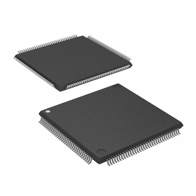
ACEX-1K® Field Programmable Gate Array (FPGA) IC 102 40960 2880 144-LQFP |
|---|---|
| Quantity | 342 Available (as of June 15, 2026) |

| Product Category | Field Programmable Gate Array (FPGA) |
|---|---|
| Manufacturer | Intel |
| Manufacturing Status | Obsolete |
| Manufacturer Standard Lead Time | Contact Us |
| Datasheet |
Specifications & Environmental
| Device Package | 144-TQFP (20x20) | Grade | Industrial | Operating Temperature | -40°C – 85°C | ||
|---|---|---|---|---|---|---|---|
| Package / Case | 144-LQFP | Number of I/O | 102 | Voltage | 2.375 V - 2.625 V | ||
| Mounting Method | Surface Mount | RoHS Compliance | RoHS non-compliant | REACH Compliance | REACH Unaffected | ||
| Moisture Sensitivity Level | 3 (168 Hours) | Number of LABs/CLBs | 360 | Number of Logic Elements/Cells | 2880 | ||
| Number of Gates | 199000 | ECCN | 3A991D | HTS Code | 8542.39.0001 | ||
| Qualification | N/A | Total RAM Bits | 40960 |
Overview of EP1K50TI144-2 – ACEX-1K® Field Programmable Gate Array (FPGA) IC 102 40960 2880 144-LQFP
The EP1K50TI144-2 is an ACEX-1K family programmable logic device (FPGA) designed for mid-density system integration. It combines a logic array with embedded array blocks (EABs) to implement both general-purpose logic and efficient on-chip memory for system-on-a-programmable-chip (SOPC) applications.
Targeted at industrial and communications-oriented designs, the device delivers a balance of logic capacity, embedded RAM, and flexible I/O capability while operating over an extended temperature range and a low-voltage internal supply.
Key Features
- Core Logic: 2,880 logic elements (LEs) providing mid-range integration for glue logic, custom peripherals, and control functions.
- Embedded Memory (EABs): Ten embedded array blocks with a total of 40,960 bits of RAM, including dual-port capability and up to 16-bit width per EAB for efficient on-chip storage and megafunction implementation.
- Gate Count: Device-level capacity up to 199,000 system gates enabling implementation of sizeable logic and system functions.
- I/O and Voltage: 102 user I/O pins with MultiVolt capability (I/O can interface with 2.5 V, 3.3 V, or 5.0 V devices) and an internal supply operating around 2.5 V (device supply range 2.375 V to 2.625 V).
- Package and Mounting: 144-pin LQFP package (supplier reference: 144-TQFP 20×20) for surface-mount board designs.
- Industrial Temperature Grade: Rated for operation from -40 °C to 85 °C for deployment in industrial environments.
- In-Circuit Reconfigurability and Test: Supports in-circuit reconfigurability via external configuration devices or JTAG; includes IEEE 1149.1-compatible boundary-scan test circuitry without consuming device logic.
- Clocking and Performance Features: Built-in low-skew clock distribution trees with ClockLock and ClockBoost options plus dedicated carry and cascade chains for arithmetic and high-fan-in logic.
- Flexible Interconnect: FastTrack continuous routing structure for predictable interconnect delays and tri-state emulation for internal bus structures.
Typical Applications
- Communications Infrastructure — Implements protocol bridging, packet processing support logic, and interface glue in networking and telecom equipment using the device's embedded RAM and dedicated arithmetic chains.
- SOPC and Custom IP Integration — Integrates megafunctions and custom peripherals, benefitting from EAB dual-port RAM and the device's reconfigurability for evolving system requirements.
- Industrial Control and Automation — Handles control logic, sensor interfacing, and deterministic I/O tasks within an industrial temperature range and low-voltage internal supply.
- Memory-intensive Logic Functions — Uses the on-chip EABs for FIFOs, lookup tables, and small embedded buffers to reduce external memory dependencies and simplify board-level design.
Unique Advantages
- Highly Integrated Mid-Density Solution: 2,880 logic elements combined with ten EABs and ~40,960 bits of embedded RAM reduce external component count and board complexity.
- Flexible I/O Voltage Support: MultiVolt I/O lets the device interface with 2.5 V, 3.3 V, or 5.0 V systems, simplifying mixed-voltage designs.
- Industrial Reliability: Rated for -40 °C to 85 °C operation, making it suitable for industrial-grade deployments.
- Reconfigurability and Testability: In-circuit reconfigurability and IEEE 1149.1-compliant JTAG boundary-scan enable field updates and board-level test without consuming user logic.
- Deterministic Clocking and Arithmetic Support: Low-skew clock trees plus dedicated carry and cascade chains accelerate arithmetic, counters, and wide combinational logic implementations.
- Predictable Routing: FastTrack interconnect structure delivers consistent routing delays for repeatable timing results across designs.
Why Choose EP1K50TI144-2?
The EP1K50TI144-2 positions itself as a versatile, mid-density FPGA for designers who need a balance of on-chip memory, deterministic logic resources, and flexible I/O. Its combination of 2,880 logic elements, ten EABs totaling 40,960 bits of RAM, and up to 199,000 system gates addresses a wide range of SOPC, communications, and industrial control tasks while supporting in-circuit reconfiguration and boundary-scan testing.
Engineers seeking a cost-efficient, industrial-grade programmable device with predictable interconnect and dedicated arithmetic resources will find the EP1K50TI144-2 suitable for accelerating development and simplifying board-level design trade-offs.
Request a quote or submit a sales inquiry to evaluate EP1K50TI144-2 for your next design and learn about available inventory and pricing.


Date Founded: 1968
Headquarters: Santa Clara, California, USA
Employees: 130,000+
Revenue: $54.23 Billion
Certifications and Memberships: ISO9001:2015, ISO14001:2015, ISO17025:2017, ISO27001:2022, ISO45001:2018, ISO50001:2018


