
EP1S10F780C7
| Part Description |
Stratix® Field Programmable Gate Array (FPGA) IC 426 920448 10570 780-BBGA |
|---|---|
| Quantity | 804 Available (as of June 17, 2026) |

| Product Category | Field Programmable Gate Array (FPGA) |
|---|---|
| Manufacturer | Intel |
| Manufacturing Status | Obsolete |
| Manufacturer Standard Lead Time | Contact Us |
| Datasheet |
Specifications & Environmental
| Device Package | 780-FBGA (29x29) | Grade | Commercial | Operating Temperature | 0°C – 85°C | ||
|---|---|---|---|---|---|---|---|
| Package / Case | 780-BBGA | Number of I/O | 426 | Voltage | 1.425 V - 1.575 V | ||
| Mounting Method | Surface Mount | RoHS Compliance | RoHS non-compliant | REACH Compliance | REACH Unaffected | ||
| Moisture Sensitivity Level | 3 (168 Hours) | Number of LABs/CLBs | 1057 | Number of Logic Elements/Cells | 10570 | ||
| Number of Gates | N/A | ECCN | 3A991D | HTS Code | 8542.39.0001 | ||
| Qualification | N/A | Total RAM Bits | 920448 |
Overview of EP1S10F780C7 – Stratix Field Programmable Gate Array, 10,570 logic elements, 780-BBGA
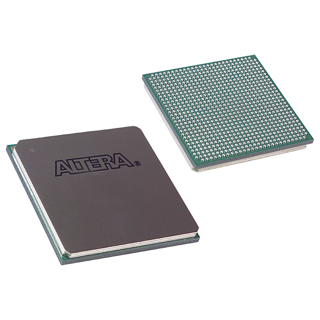
The EP1S10F780C7 is a Stratix® Field Programmable Gate Array (FPGA) from Intel presented in a 780‑ball BGA package. This commercial‑grade, surface‑mount FPGA provides 10,570 logic elements and approximately 0.92 Mbits of on‑chip RAM, with a 426‑pin I/O capability for high‑pin‑count system designs.
Designed around the Stratix family architecture described in the device handbook, the device combines configurable logic, embedded memory, and advanced I/O and clocking capabilities to support system integration tasks where a high I/O count, on‑chip memory, and a compact BGA package are required. Electrical operation is supported across a core supply window of 1.425 V to 1.575 V and a commercial operating temperature range of 0 °C to 85 °C.
Key Features
- Core Logic 10,570 logic elements to implement combinational and sequential logic functions for complex digital designs.
- Embedded Memory Approximately 0.92 Mbits of on‑chip RAM for buffering, FIFOs, and small data-store functions without external memory.
- I/O Density 426 I/O pins enable dense peripheral and board‑level connectivity for multi‑lane interfaces and parallel buses.
- Power and Voltage Core supply specified from 1.425 V to 1.575 V to match system power rails and sequencing requirements.
- Package and Mounting 780‑BBGA package (supplier device package: 780‑FBGA, 29×29) in a surface‑mount form factor for compact PCB integration.
- Operating Grade Commercial grade with an operating temperature range of 0 °C to 85 °C suitable for standard industrial and commercial applications.
- Stratix Family Capabilities (per device handbook) Architecture documentation for the Stratix family covers logic array blocks, memory modes, multiplier/DSP block interfaces, PLLs and clock networks, and advanced I/O, providing a platform of established FPGA features for system designers.
- Environmental Compliance RoHS‑compliant construction for alignment with common environmental requirements.
Typical Applications
- High‑Density Logic Prototyping Use the device’s 10,570 logic elements and substantial I/O count to implement board‑level prototypes and validate complex logic before production.
- Data and Signal Processing Embedded RAM and the Stratix family’s documented multiplier/DSP interfaces support buffering and localized processing tasks.
- Interface and Protocol Bridging A large number of I/O pins makes the device suitable for designs that require multiple parallel interfaces or protocol translation between subsystems.
- Embedded System Integration On‑chip memory and configurable logic let designers consolidate glue logic and small data‑path functions into a single packaged FPGA.
Unique Advantages
- Substantial Logic Capacity: 10,570 logic elements enable implementation of complex control and data‑path functions without immediate need for additional programmable devices.
- High I/O Count: 426 I/O pins reduce external interface multiplexing and simplify routing for multi‑lane or multi‑bus designs.
- Integrated On‑Chip Memory: Approximately 0.92 Mbits of embedded RAM provides local storage for FIFOs, buffers, and small data structures, lowering dependence on external memory for some use cases.
- Compact BGA Packaging: 780‑ball BGA (29×29 supplier package) offers a space‑efficient footprint for high‑density boards and surface‑mount assembly.
- Documented Stratix Architecture: Family handbook chapters covering clocking, memory modes, and I/O structure provide design guidance and architectural features to leverage in system designs.
- Regulatory Readiness: RoHS compliance simplifies environmental qualification and procurement in many regions.
Why Choose EP1S10F780C7?
The EP1S10F780C7 positions itself as a Stratix‑family FPGA option for designers who need a balance of logic density, embedded memory, and a high I/O count in a compact BGA package. Its documented Stratix architecture and on‑chip resources make it suitable for consolidating control, interfacing, and moderate‑complexity processing tasks into a single device.
This part is appropriate for commercial applications requiring a surface‑mount FPGA with a 1.425 V–1.575 V core supply and a 0 °C–85 °C operating range. The combination of logic elements, embedded RAM, and extensive I/O supports scalable designs and reduces external component count for many system integration scenarios.
Request a quote or submit an inquiry for pricing and availability of EP1S10F780C7 to evaluate this Stratix FPGA for your next design.


Date Founded: 1968
Headquarters: Santa Clara, California, USA
Employees: 130,000+
Revenue: $54.23 Billion
Certifications and Memberships: ISO9001:2015, ISO14001:2015, ISO17025:2017, ISO27001:2022, ISO45001:2018, ISO50001:2018


