
EP1S20F484C7N
| Part Description |
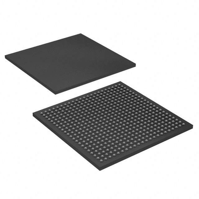
Stratix® Field Programmable Gate Array (FPGA) IC 361 1669248 18460 484-BBGA, FCBGA |
|---|---|
| Quantity | 854 Available (as of June 14, 2026) |

| Product Category | Field Programmable Gate Array (FPGA) |
|---|---|
| Manufacturer | Intel |
| Manufacturing Status | Obsolete |
| Manufacturer Standard Lead Time | Contact Us |
| Datasheet |
Specifications & Environmental
| Device Package | 484-FBGA (23x23) | Grade | Commercial | Operating Temperature | 0°C – 85°C | ||
|---|---|---|---|---|---|---|---|
| Package / Case | 484-BBGA, FCBGA | Number of I/O | 361 | Voltage | 1.425 V - 1.575 V | ||
| Mounting Method | Surface Mount | RoHS Compliance | Unknown | REACH Compliance | REACH Unaffected | ||
| Moisture Sensitivity Level | 3 (168 Hours) | Number of LABs/CLBs | 1846 | Number of Logic Elements/Cells | 18460 | ||
| Number of Gates | N/A | ECCN | 3A001A7A | HTS Code | 8542.39.0001 | ||
| Qualification | N/A | Total RAM Bits | 1669248 |
Overview of EP1S20F484C7N – Stratix Field Programmable Gate Array (FPGA) IC, 18,460 logic elements
The EP1S20F484C7N is a Stratix family Field Programmable Gate Array (FPGA) in a 484-ball BGA (FCBGA) package. It provides a large logic resource and a substantial on-chip memory footprint for system integration in commercial applications.
With 18,460 logic elements, approximately 1.669 Mbits of embedded memory and 361 I/O pins, this device targets designs that require significant logic capacity, high I/O density and flexible configuration and clocking features provided by the Stratix architecture.
Key Features
- Core Logic 18,460 logic elements for implementing complex digital logic and programmable functions consistent with the Stratix device family architecture.
- Embedded Memory Approximately 1.669 Mbits of on-chip RAM bits to support buffering, caching and logic-local storage requirements.
- I/O Density & Flexibility 361 user I/Os to support broad interfacing needs; the Stratix family documentation details advanced I/O features including high-speed differential I/O support and programmable drive options.
- Clocking & Timing Family-level support for PLLs and advanced clock networks provides flexible clock management and distribution for synchronous designs.
- Configuration & Debug Stratix device handbook describes configuration schemes including JTAG (IEEE 1149.1) boundary-scan support, SignalTap II embedded logic analyzer and options for partial reconfiguration.
- Power Supply Operates with a core voltage supply range of 1.425 V to 1.575 V as specified for this device.
- Package & Mounting Surface-mount 484-BBGA (FCBGA) package—supplier package designated 484-FBGA (23×23)—enables high-density board integration.
- Commercial Temperature Grade Rated for commercial operation from 0 °C to 85 °C.
- Standards & Design Resources The Stratix device handbook provides extensive architecture, timing, I/O and configuration documentation to support system design and validation.
Typical Applications
- Communications Equipment Use for applications requiring high I/O counts and advanced clocking—suitable where substantial programmable logic and memory are needed for data path implementation.
- Signal Processing & DSP Appropriate for designs that leverage the Stratix family’s multiplier/DSP blocks and embedded memory to implement filtering, aggregation or other data-processing functions.
- Prototyping & System Integration Useful in development platforms and proof-of-concept systems that require significant logic capacity and flexible configuration options including in-system debug.
- Test & Measurement High I/O density and on-chip resources make the device suitable for instrumentation, capture and custom protocol handling.
Unique Advantages
- Large Logic Capacity: 18,460 logic elements allow consolidation of multiple functions into a single device, reducing board complexity.
- Substantial On-Chip Memory: Approximately 1.669 Mbits of embedded RAM supports local buffering and state storage without external memory for many use cases.
- High I/O Count: 361 I/O pins enable dense external connectivity for multi-channel interfaces and parallel buses.
- Flexible Clocking & Configuration: Family features such as PLLs, advanced clock networks, JTAG boundary-scan and SignalTap II support integrated timing control and in-system debug.
- Commercial Temperature & Industry Documentation: Commercial-grade temperature range (0 °C to 85 °C) and comprehensive Stratix handbook content help streamline design and validation.
- Compact Surface-Mount Packaging: 484-BBGA (484-FBGA 23×23) package supports compact board layouts while delivering high I/O density.
Why Choose EP1S20F484C7N?
The EP1S20F484C7N combines significant programmable logic, embedded memory and a high I/O count in a commercial-grade Stratix FPGA package. It is well-suited for engineers and designers who need a high-capacity, configurable device with robust family-level features for clocking, configuration and in-system debug.
Backed by the Stratix device handbook and family documentation, this part delivers a documented platform for scalable designs where integration, flexibility and maintainability are priorities.
Request a quote or submit a quote to obtain pricing and availability for EP1S20F484C7N.


Date Founded: 1968
Headquarters: Santa Clara, California, USA
Employees: 130,000+
Revenue: $54.23 Billion
Certifications and Memberships: ISO9001:2015, ISO14001:2015, ISO17025:2017, ISO27001:2022, ISO45001:2018, ISO50001:2018


