
EP1S20F484C5N
| Part Description |
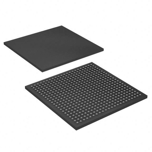
Stratix® Field Programmable Gate Array (FPGA) IC 361 1669248 18460 484-BBGA, FCBGA |
|---|---|
| Quantity | 216 Available (as of June 14, 2026) |

| Product Category | Field Programmable Gate Array (FPGA) |
|---|---|
| Manufacturer | Intel |
| Manufacturing Status | Obsolete |
| Manufacturer Standard Lead Time | Contact Us |
| Datasheet |
Specifications & Environmental
| Device Package | 484-FBGA (23x23) | Grade | Commercial | Operating Temperature | 0°C – 85°C | ||
|---|---|---|---|---|---|---|---|
| Package / Case | 484-BBGA, FCBGA | Number of I/O | 361 | Voltage | 1.425 V - 1.575 V | ||
| Mounting Method | Surface Mount | RoHS Compliance | Unknown | REACH Compliance | REACH Unaffected | ||
| Moisture Sensitivity Level | 3 (168 Hours) | Number of LABs/CLBs | 1846 | Number of Logic Elements/Cells | 18460 | ||
| Number of Gates | N/A | ECCN | 3A001A7A | HTS Code | 8542.39.0001 | ||
| Qualification | N/A | Total RAM Bits | 1669248 |
Overview of EP1S20F484C5N – Stratix® FPGA, 18,460 logic elements, ~1.67 Mbits RAM, 361 I/Os
The EP1S20F484C5N is a Stratix® family field programmable gate array (FPGA) supplied in a 484‑FBGA surface‑mount package. It integrates 18,460 logic elements, approximately 1.67 Mbits of on‑chip RAM, and 361 general‑purpose I/Os to support complex, programmable digital designs.
Built on the Stratix architecture, this device provides the building blocks referenced in the Stratix device handbook—including programmable logic array structures, embedded memory structures, PLLs and advanced I/O options—positioning it for demanding digital, timing‑sensitive applications within commercial temperature ranges.
Key Features
- Logic Capacity 18,460 logic elements for implementing glue logic, state machines, and custom datapaths.
- Embedded Memory Approximately 1.67 Mbits of on‑chip RAM for frame buffers, FIFOs, and local storage.
- I/O Resources 361 I/O pins to support broad peripheral interfacing and multi‑lane I/O topologies; the Stratix device family documentation includes support for high‑speed differential I/O and advanced I/O standards.
- Clocking & Timing Supports Stratix PLLs and clocking networks as described in the device handbook for flexible clock management and hierarchical clocking strategies.
- DSP & Math Support Device family architecture includes multiplier and DSP block interfaces suitable for implementing signal processing pipelines and arithmetic‑intensive logic.
- Configuration & Test Features Series documentation references IEEE Std. 1149.1 (JTAG) boundary‑scan support, SignalTap II embedded logic analyzer functionality, and multiple configuration options including partial reconfiguration.
- Package & Power Surface‑mount 484‑BBGA / FCBGA (supplier package: 484‑FBGA 23×23) with an operating core supply range of 1.425 V–1.575 V.
- Commercial Temperature Grade Rated for operation from 0 °C to 85 °C and RoHS compliant.
Typical Applications
- High‑speed data acquisition and processing Use the device’s DSP block interfaces, embedded RAM, and high‑performance I/O support to implement capture, buffering, and preprocessing pipelines.
- Memory interfacing and buffering On‑chip RAM combined with external RAM interfacing capability (described in the device handbook) makes it suitable for designs requiring local buffering and external memory controllers.
- Custom logic and prototyping The programmable array of logic elements and flexible clocking architecture enable rapid prototyping of custom controllers, protocol bridges, and system glue logic.
Unique Advantages
- Substantial logic density: 18,460 logic elements provide the capacity to integrate multiple functions and reduce board‑level component count.
- Generous embedded memory: Approximately 1.67 Mbits of on‑chip RAM supports local buffering and state storage, lowering external memory bandwidth needs.
- Wide I/O count: 361 I/Os enable flexible system partitioning and direct connection to peripherals, sensors, and parallel interfaces.
- Comprehensive clocking resources: Stratix PLLs and hierarchical clocking (documented in the device handbook) help manage multi‑domain timing and maximize performance headroom.
- Built‑in test and configuration capabilities: JTAG boundary‑scan and embedded logic analysis options simplify bring‑up, debug, and in‑system reconfiguration workflows.
- Commercial‑grade and RoHS compliant: Designed for commercial temperature environments (0 °C to 85 °C) and compliant with RoHS requirements.
Why Choose EP1S20F484C5N?
The EP1S20F484C5N offers a balanced combination of logic capacity, embedded memory, and I/O resources within a compact 484‑FBGA package—making it suitable for designers who need programmable logic density and on‑chip storage while staying within commercial temperature ranges. Its inclusion in the Stratix device family provides access to proven architectural features such as advanced clocking, DSP interfaces, and the configuration and test capabilities detailed in the device handbook.
This device is appropriate for engineers and procurement teams building medium‑ to high‑complexity digital systems requiring flexible programmability, local memory, and broad I/O connectivity, backed by the documented Stratix architecture and development ecosystem.
Request a quote or submit a quote for EP1S20F484C5N to get pricing and availability information for your next design.


Date Founded: 1968
Headquarters: Santa Clara, California, USA
Employees: 130,000+
Revenue: $54.23 Billion
Certifications and Memberships: ISO9001:2015, ISO14001:2015, ISO17025:2017, ISO27001:2022, ISO45001:2018, ISO50001:2018


