
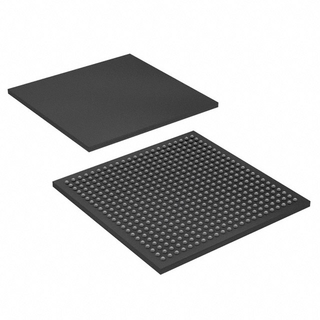
EP1S20F484C5
| Part Description |
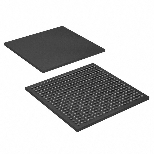
Stratix® Field Programmable Gate Array (FPGA) IC 361 1669248 18460 484-BBGA, FCBGA |
|---|---|
| Quantity | 1,191 Available (as of October 8, 2026) |
| Product Category | Field Programmable Gate Array (FPGA) |
|---|---|
| Manufacturer | Intel |
| Manufacturing Status | Obsolete |
| Manufacturer Standard Lead Time | Contact Us |
| Datasheet |
Specifications & Environmental
| Device Package | 484-FBGA (23x23) | Grade | Commercial | Operating Temperature | 0°C – 85°C | ||
|---|---|---|---|---|---|---|---|
| Package / Case | 484-BBGA, FCBGA | Number of I/O | 361 | Voltage | 1.425 V - 1.575 V | ||
| Mounting Method | Surface Mount | RoHS Compliance | RoHS non-compliant | REACH Compliance | REACH Unaffected | ||
| Moisture Sensitivity Level | 3 (168 Hours) | Number of LABs/CLBs | 1846 | Number of Logic Elements/Cells | 18460 | ||
| Number of Gates | N/A | ECCN | 3A001A7A | HTS Code | 8542.39.0001 | ||
| Qualification | N/A | Total RAM Bits | 1669248 |
Overview of EP1S20F484C5 – Stratix® Field Programmable Gate Array (FPGA) IC, 18,460 logic elements
The EP1S20F484C5 is a Stratix® series FPGA in a 484-ball FCBGA package designed for commercial embedded and enterprise applications. It combines a high logic element count with on-chip memory and a large I/O complement to support complex digital designs and high-density interfacing.
Built on the Stratix device architecture, this device addresses use cases that require flexible logic implementation, on-chip RAM, and comprehensive I/O capability—delivering integration and configurability for system designers.
Key Features
- Logic Capacity Provides 18,460 logic elements suitable for medium-to-large custom logic integration and glue logic within a single FPGA.
- Embedded Memory Approximately 1.67 Mbits of on-chip RAM to support FIFOs, buffers, and local storage for data-path and control logic.
- I/O Density 361 I/O pins to support broad interfacing requirements, including parallel buses and external device connections.
- Package & Mounting 484-BBGA (FCBGA) surface-mount package (484-FBGA, 23×23) for high-density board designs and reliable soldered mounting.
- Power Operates from a core supply range of 1.425 V to 1.575 V, enabling predictable integration into regulated power systems.
- Operating Range & Grade Commercial grade device with an operating temperature range of 0 °C to 85 °C and RoHS compliance for environmental requirements.
- Configuration & Test Support Stratix family features shown in the device handbook include JTAG (IEEE 1149.1) boundary-scan support and embedded logic analysis and configuration options for development and debug.
- Clocking & DSP-Related Resources Stratix device documentation references PLLs, global clocking networks, multiplier blocks, and DSP block interfaces to support timing and signal-processing design patterns.
Typical Applications
- Custom Data-Path Acceleration Implement algorithmic acceleration and custom hardware pipelines using the device’s logic elements and on-chip RAM for intermediate storage.
- High-Density I/O Bridging Use the 361 I/O pins to connect to multiple buses, serializers/deserializers, or parallel interfaces in communication and interface conversion roles.
- Prototyping and Platform Development Leverage the Stratix architecture and configuration/test features for hardware/software co-design, verification, and iterative development.
- Digital Signal Processing Exploit the documented multiplier and DSP block interfaces in the Stratix family for signal processing tasks requiring dedicated arithmetic resources.
Unique Advantages
- High logic integration: 18,460 logic elements let you consolidate multiple discrete functions into a single programmable device, reducing board-level complexity.
- Significant on-chip memory: Approximately 1.67 Mbits of embedded RAM supports buffering, packet queuing, and local data storage without external memory.
- Broad I/O capability: 361 I/O pins provide flexibility for multi-board systems, parallel interfaces, and mixed-signal front-ends.
- Commercial operating range: Rated for 0 °C to 85 °C, suited to a wide range of commercial and enterprise deployment environments.
- Standards-based configuration and debug: Documented support for JTAG boundary-scan and embedded logic analysis aids development, testing, and in-field diagnostics.
- RoHS compliant: Conforms to RoHS environmental requirements for regulatory and supply-chain consistency.
Why Choose EP1S20F484C5?
The EP1S20F484C5 offers a balanced mix of logic density, embedded memory, and I/O capacity in a compact 484-ball FCBGA package, making it a strong choice for designers who need integrated digital resources without resorting to multiple discrete devices. Its documented Stratix family features—clocking resources, multiplier/DSP interfaces, and configuration/test capabilities—support robust system-level design and verification workflows.
This device is well suited to teams developing commercial embedded systems, platform prototypes, and hardware-accelerated functions where on-chip RAM, abundant I/O, and a known configuration ecosystem deliver long-term design scalability and predictable integration.
Request a quote or submit an inquiry to receive pricing, availability, and assistance integrating the EP1S20F484C5 into your next design.






















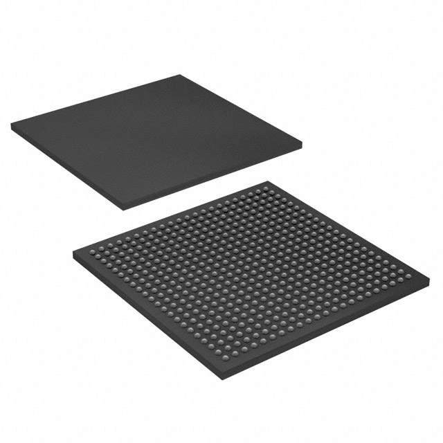

Date Founded: 1968
Headquarters: Santa Clara, California, USA
Employees: 130,000+
Revenue: $54.23 Billion
Certifications and Memberships: ISO9001:2015, ISO14001:2015, ISO17025:2017, ISO27001:2022, ISO45001:2018, ISO50001:2018


