
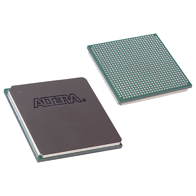
EP1S25F780C5
| Part Description |
Stratix® Field Programmable Gate Array (FPGA) IC 597 1944576 25660 780-BBGA |
|---|---|
| Quantity | 1,031 Available (as of June 18, 2026) |

| Product Category | Field Programmable Gate Array (FPGA) |
|---|---|
| Manufacturer | Intel |
| Manufacturing Status | Obsolete |
| Manufacturer Standard Lead Time | Contact Us |
| Datasheet |
Specifications & Environmental
| Device Package | 780-FBGA (29x29) | Grade | Commercial | Operating Temperature | 0°C – 85°C | ||
|---|---|---|---|---|---|---|---|
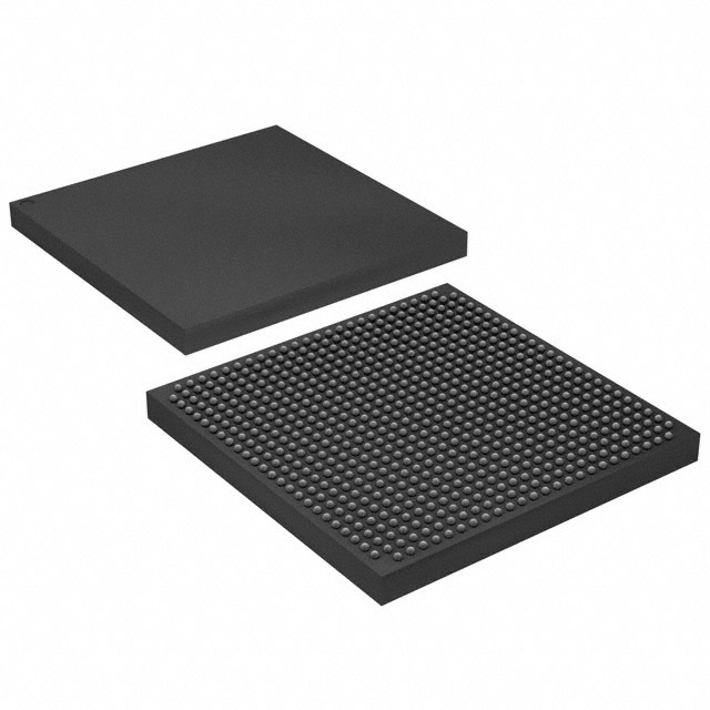
| Package / Case | 780-BBGA | Number of I/O | 597 | Voltage | 1.425 V - 1.575 V | ||
| Mounting Method | Surface Mount | RoHS Compliance | RoHS non-compliant | REACH Compliance | REACH Unaffected | ||
| Moisture Sensitivity Level | 3 (168 Hours) | Number of LABs/CLBs | 2566 | Number of Logic Elements/Cells | 25660 | ||
| Number of Gates | N/A | ECCN | 3A001A7A | HTS Code | 8542.39.0001 | ||
| Qualification | N/A | Total RAM Bits | 1944576 |
Overview of EP1S25F780C5 – Stratix FPGA, 25,660 logic elements, ~1.94 Mbits RAM, 597 I/Os, 780-BBGA
The EP1S25F780C5 is a Stratix® Field Programmable Gate Array (FPGA) IC from Intel, delivering a substantial pool of configurable logic and on-chip memory in a 780-ball BGA package. Built on the Stratix device architecture, this device targets designs that require dense logic resources, significant embedded RAM, flexible I/O, and advanced clocking and DSP support described in the Stratix device handbook.
This commercial-grade FPGA is suited for applications that need programmable system integration, multi-clock domains and high I/O counts while operating within a 0 °C to 85 °C temperature range and a core supply window of 1.425 V to 1.575 V.
Key Features
- Core Logic 25,660 logic elements provide a large capacity for implementing custom digital logic, state machines and control functions.
- Embedded Memory Approximately 1.94 Mbits of on-chip RAM support buffering, FIFOs and lookup tables, with Stratix memory modes and TriMatrix memory architecture referenced in the device handbook.
- I/O Resources 597 user I/O pins accommodate wide parallel interfaces and large external connectivity requirements; the Stratix family documentation includes support for high-speed differential and DDR I/O modes.
- Clocking and Timing Stratix PLLs and clock network capabilities (including enhanced and fast PLLs) enable complex clocking schemes and multi-clock domain designs.
- DSP and Arithmetic Blocks Device-level support for multiplier blocks and DSP block interfaces provides building blocks for signal processing and arithmetic acceleration.
- Configuration & Test Stratix family features such as IEEE 1149.1 JTAG boundary-scan and on-device logic analysis (SignalTap II) are described in the device handbook for configuration and debug workflows.
- Power & Electrical Core supply voltage range is 1.425 V to 1.575 V, enabling integration into systems with tight supply specifications.
- Package & Mounting 780-BBGA package (supplier device package: 780-FBGA, 29 × 29 mm) with surface-mount assembly for dense board-level integration.
- Grade & Environmental Commercial grade device, RoHS compliant, with operating temperature from 0 °C to 85 °C.
Typical Applications
- High-speed I/O interfaces — Use the high I/O count and Stratix I/O capabilities to implement interface bridging, parallel buses and DDR signaling.
- Memory buffering and packet processing — Approximately 1.94 Mbits of embedded RAM and configurable memory modes support buffering, FIFO and packet buffering tasks.
- DSP and algorithm acceleration — Multiplier and DSP block interfaces described for the Stratix family enable fixed-point and streaming signal-processing blocks.
- System prototyping and integration — Large logic capacity and advanced clocking resources support complex custom logic, protocol consolidation and multi-clock designs.
Unique Advantages
- High logic density: 25,660 logic elements provide the capacity to implement large, integrated digital functions on a single device, reducing BOM and board count.
- Substantial embedded memory: Approximately 1.94 Mbits of on-chip RAM enables local buffering and memory-heavy functions without immediate external memory dependence.
- Extensive I/O: 597 I/Os support broad connectivity for wide buses, parallel interfaces and multi-channel systems.
- Family-level clocking and DSP support: Stratix device architecture includes PLLs, clock networks and DSP/multiplier blocks for implementing multi-clock and signal-processing systems.
- Package integration: The 780-BBGA (780-FBGA, 29 × 29 mm) package provides a compact, surface-mount solution for dense PCB implementations.
- Compliance and commercial readiness: RoHS compliant and specified for 0 °C to 85 °C operation to meet typical commercial deployment requirements.
Why Choose EP1S25F780C5?
The EP1S25F780C5 combines a high count of logic elements, meaningful on-chip RAM and a very large I/O complement in a single commercial-grade Stratix FPGA. Its specification set—core voltage range, package format and documented Stratix architecture features such as PLLs, DSP blocks and advanced I/O—makes it a practical choice for designers consolidating complex digital functions and high-bandwidth interfaces onto one programmable device.
This device is well suited to teams building high-density digital systems, memory-buffering engines, protocol bridges and signal-processing blocks who need a configurable platform with established family-level architecture and tooling described in the Stratix device handbook.
Request a quote or submit an inquiry to evaluate EP1S25F780C5 for your next design and to receive availability and pricing information.


Date Founded: 1968
Headquarters: Santa Clara, California, USA
Employees: 130,000+
Revenue: $54.23 Billion
Certifications and Memberships: ISO9001:2015, ISO14001:2015, ISO17025:2017, ISO27001:2022, ISO45001:2018, ISO50001:2018


