
EP1S25F672I7N
| Part Description |
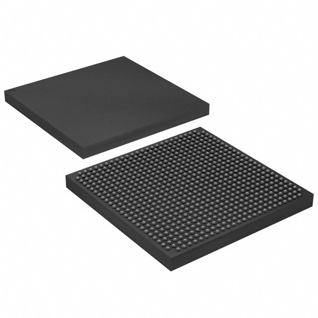
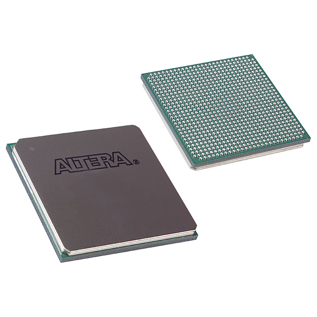
Stratix® Field Programmable Gate Array (FPGA) IC 473 1944576 25660 672-BBGA |
|---|---|
| Quantity | 1,522 Available (as of June 16, 2026) |

| Product Category | Field Programmable Gate Array (FPGA) |
|---|---|
| Manufacturer | Intel |
| Manufacturing Status | Obsolete |
| Manufacturer Standard Lead Time | Contact Us |
| Datasheet |
Specifications & Environmental
| Device Package | 672-FBGA (27x27) | Grade | Industrial | Operating Temperature | -40°C – 100°C | ||
|---|---|---|---|---|---|---|---|
| Package / Case | 672-BBGA | Number of I/O | 473 | Voltage | 1.425 V - 1.575 V | ||
| Mounting Method | Surface Mount | RoHS Compliance | Unknown | REACH Compliance | REACH Unaffected | ||
| Moisture Sensitivity Level | 3 (168 Hours) | Number of LABs/CLBs | 2566 | Number of Logic Elements/Cells | 25660 | ||
| Number of Gates | N/A | ECCN | 3A991D | HTS Code | 8542.39.0001 | ||
| Qualification | N/A | Total RAM Bits | 1944576 |
Overview of EP1S25F672I7N – Stratix FPGA IC, 672‑BBGA
The EP1S25F672I7N is a Stratix® field‑programmable gate array (FPGA) from Intel (Altera) supplied in a 672‑ball BGA package. It provides a programmable logic fabric and on‑chip resources designed for complex digital systems requiring flexible I/O, embedded memory, and high‑performance logic integration.
With approximately 25,660 logic elements and about 1.94 Mbits of embedded memory, this industrial‑grade device targets designs that require substantial on‑chip logic capacity, extensive I/O count, and robust operating conditions.
Key Features
- Logic Capacity — Approximately 25,660 logic elements provide the programmable resources for implementing complex state machines, datapaths, and custom logic functions.
- Embedded Memory — Approximately 1.94 Mbits of on‑chip RAM (total RAM bits: 1,944,576) for frame buffers, FIFOs, and local storage to support high‑performance datapaths.
- I/O Resources — 473 I/O pins to support wide parallel interfaces and multiple high‑speed links as required by system designs.
- Stratix Architecture Features — Device handbook topics include logic array blocks, LUT/register chains, multiplier and DSP block interfaces, PLLs and clock networks, and advanced I/O support such as double‑data‑rate pins and high‑speed differential I/O.
- Configuration & Debug — Supports standard configuration and testing features referenced in the Stratix handbook, including JTAG boundary‑scan and embedded logic analyzer capabilities for in‑system debug and verification.
- Power Supply — Core supply specified at 1.425 V to 1.575 V to match system power rails and ensure predictable device operation.
- Package & Mounting — 672‑BBGA (supplier package: 672‑FBGA, 27×27 mm) in a surface‑mount form factor suitable for compact, board‑level integration.
- Industrial Temperature Grade — Rated for operation from −40 °C to 100 °C, supporting deployment in industrial environments.
- Regulatory — RoHS compliant.
Typical Applications
- High‑performance digital processing — Implement datapath acceleration, custom arithmetic, and DSP functions using the device’s logic elements, multipliers, and DSP block interfaces.
- Memory interface and buffering — Use the approximately 1.94 Mbits of embedded RAM and memory modes described in the Stratix handbook for external RAM interfacing and on‑chip buffering.
- Multi‑lane I/O systems — Leverage 473 I/Os and high‑speed differential I/O support for wide parallel buses, multi‑channel interfaces, and DDR signaling.
- Clocking‑sensitive designs — Deploy the device’s PLLs, global and hierarchical clocking features to manage multiple clock domains and achieve deterministic timing for synchronous systems.
Unique Advantages
- Substantial logic and memory in one device: Approximately 25,660 logic elements combined with ~1.94 Mbits of embedded memory reduce the need for external glue logic and local RAM, simplifying board design.
- Extensive I/O connectivity: 473 I/O pins enable wide interfaces and flexible pin assignment for complex peripheral and bus integrations.
- Industrial temperature range: Rated from −40 °C to 100 °C, supporting deployment in environments requiring extended thermal tolerance.
- Proven Stratix architecture: Architectural elements such as dedicated multiplier/DSP interfaces, PLLs, and advanced I/O constructs (as documented in the Stratix handbook) provide design building blocks for timing‑critical and compute‑intensive applications.
- Compact BGA packaging: 672‑ball BGA (27×27 mm) enables high‑density board layouts while maintaining compatibility with standard surface‑mount assembly practices.
- Standards‑oriented test and debug: On‑device support for JTAG boundary‑scan and embedded logic analysis assists in validation, in‑system testing, and failure diagnosis during development and production.
Why Choose EP1S25F672I7N?
The EP1S25F672I7N positions itself as a robust Stratix FPGA option for designs that require a balance of high logic capacity, substantial on‑chip memory, and broad I/O resources in an industrial‑temperature package. Its architecture—documented in the Stratix device handbook—includes DSP and multiplier resources, flexible memory modes, and comprehensive clocking features to support demanding digital systems.
This device suits engineering teams building compute‑intensive modules, custom interfaces, and systems that demand reliable operation across extended temperature ranges. Selecting the EP1S25F672I7N delivers a scalable, field‑programmable platform backed by Intel/Altera’s Stratix architecture and documented device features.
Request a quote or submit an inquiry to begin sourcing the EP1S25F672I7N for your next FPGA‑based design. Technical and procurement teams can request pricing, availability, and lead‑time details to proceed with evaluation or production planning.


Date Founded: 1968
Headquarters: Santa Clara, California, USA
Employees: 130,000+
Revenue: $54.23 Billion
Certifications and Memberships: ISO9001:2015, ISO14001:2015, ISO17025:2017, ISO27001:2022, ISO45001:2018, ISO50001:2018


