
EP1S40F780C5
| Part Description |
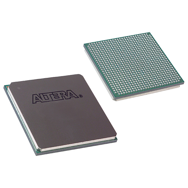
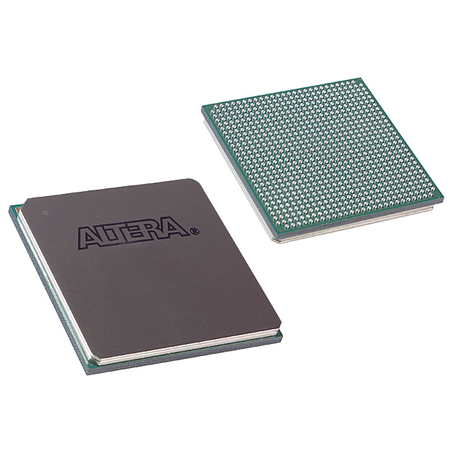
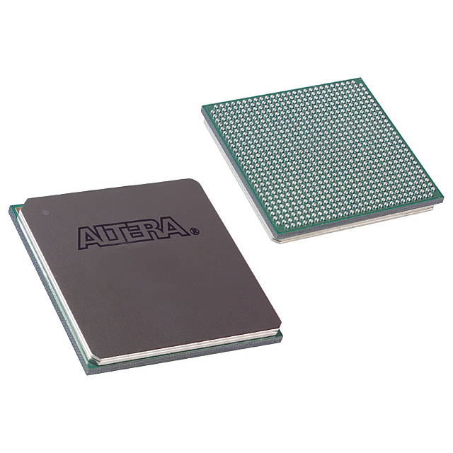
Stratix® Field Programmable Gate Array (FPGA) IC 615 3423744 41250 780-BBGA, FCBGA |
|---|---|
| Quantity | 806 Available (as of October 7, 2026) |

| Product Category | Field Programmable Gate Array (FPGA) |
|---|---|
| Manufacturer | Intel |
| Manufacturing Status | Obsolete |
| Manufacturer Standard Lead Time | Contact Us |
| Datasheet |
Specifications & Environmental
| Device Package | 780-FBGA (29x29) | Grade | Commercial | Operating Temperature | 0°C – 85°C | ||
|---|---|---|---|---|---|---|---|
| Package / Case | 780-BBGA, FCBGA | Number of I/O | 615 | Voltage | 1.425 V - 1.575 V | ||
| Mounting Method | Surface Mount | RoHS Compliance | RoHS non-compliant | REACH Compliance | REACH Unaffected | ||
| Moisture Sensitivity Level | 3 (168 Hours) | Number of LABs/CLBs | 4125 | Number of Logic Elements/Cells | 41250 | ||
| Number of Gates | N/A | ECCN | 3A001A7A | HTS Code | 8542.39.0001 | ||
| Qualification | N/A | Total RAM Bits | 3423744 |
Overview of EP1S40F780C5 – Stratix FPGA, 780‑FBGA (29×29)
The EP1S40F780C5 is a Stratix® Field Programmable Gate Array (FPGA) IC from Intel (Altera) offering high logic density and extensive I/O capability in a 780‑ball FCBGA package. It is built on the Stratix device family architecture described in the Stratix Device Handbook.
With 41,250 logic elements, approximately 3.42 Mbits of embedded RAM, and 615 I/O pins, this device is suited for designs that require significant on‑chip logic and memory resources combined with broad external interfacing and flexible clocking resources.
Key Features
- Core Logic 41,250 logic elements (Number Of Logic Elements Cells: 41250) to implement complex digital logic and custom processing blocks.
- Embedded Memory Approximately 3.42 Mbits of on‑chip RAM (Total Ram Bits: 3,423,744) with Stratix memory architecture and TriMatrix memory modes described in the device handbook.
- I/O Capacity 615 I/O pins (Number Of Io: 615) supporting advanced I/O standards, double‑data‑rate interfaces, differential signaling, and programmable I/O features referenced in the device documentation.
- Clocking & DSP Support Integrated PLLs and clock networks, enhanced and fast PLL options, and DSP block interface functionality are detailed in the Stratix handbook for timing, clocking, and signal processing use cases.
- Configuration & Debug Supports IEEE 1149.1 (JTAG) boundary‑scan, SignalTap II embedded logic analyzer, multiple configuration schemes and partial reconfiguration methods as documented for the Stratix family.
- Package, Power & Mounting 780‑BBGA FCBGA package (Supplier Device Package: 780‑FBGA (29×29)), surface‑mount mounting type, and a core voltage supply range of 1.425 V to 1.575 V.
- Operating Conditions & Compliance Commercial grade device with an operating temperature range of 0 °C to 85 °C and RoHS compliance.
Typical Applications
- High‑density digital processing — Implement complex state machines, protocol engines, and custom logic using the device’s 41,250 logic elements and embedded memory.
- High‑I/O system interfaces — Use the 615 I/O pins and advanced I/O capabilities for bridging, aggregation, or multi‑lane interface applications requiring flexible signaling options.
- On‑chip buffering and packet memory — Leverage approximately 3.42 Mbits of embedded RAM for buffering, packet queues, and other temporary storage needs without external memory.
- Clocked DSP and timing‑sensitive designs — Built‑in PLLs, clock networks, and DSP block interfaces support designs with stringent clocking and arithmetic requirements.
Unique Advantages
- Large logic capacity: 41,250 logic elements enable implementation of sizable digital designs without immediate partitioning across multiple devices.
- Substantial on‑chip memory: Approximately 3.42 Mbits of embedded RAM reduces dependency on external memory for many buffering and data‑storage functions.
- Extensive external connectivity: 615 I/Os provide broad system interfacing options for multi‑port and multi‑channel applications.
- Comprehensive clocking and DSP support: Documented PLLs, clock networks, and DSP interfaces help address timing, synchronization, and arithmetic-heavy tasks.
- Compact FCBGA footprint: 780‑FBGA (29×29) package with surface‑mount mounting supports high‑density board designs while maintaining manufacturability.
- Commercial‑grade reliability and compliance: Rated for 0 °C to 85 °C operation and RoHS compliant for standard commercial applications.
Why Choose EP1S40F780C5?
The EP1S40F780C5 positions itself as a high‑capacity Stratix FPGA option for commercial designs that require a balance of large logic resources, significant embedded memory, and extensive I/O. Its feature set—detailed in the Stratix Device Handbook—includes advanced clocking, DSP interfaces, and configuration/debug capabilities that support sophisticated FPGA implementations.
This device is a strong fit for engineering teams building systems that need on‑chip processing, buffering, and flexible external interfacing in a compact FCBGA package, backed by the Stratix device family documentation and configuration options.
Request a quote or submit a pricing inquiry to receive availability and pricing information for the EP1S40F780C5.
























Date Founded: 1968
Headquarters: Santa Clara, California, USA
Employees: 130,000+
Revenue: $54.23 Billion
Certifications and Memberships: ISO9001:2015, ISO14001:2015, ISO17025:2017, ISO27001:2022, ISO45001:2018, ISO50001:2018


