
EP1SGX25DF1020C6N
| Part Description |
Stratix® GX Field Programmable Gate Array (FPGA) IC 607 1944576 25660 1020-BBGA |
|---|---|
| Quantity | 514 Available (as of June 15, 2026) |

| Product Category | Field Programmable Gate Array (FPGA) |
|---|---|
| Manufacturer | Intel |
| Manufacturing Status | Obsolete |
| Manufacturer Standard Lead Time | Contact Us |
| Datasheet |
Specifications & Environmental
| Device Package | 1020-FBGA (33x33) | Grade | Commercial | Operating Temperature | 0°C – 85°C | ||
|---|---|---|---|---|---|---|---|
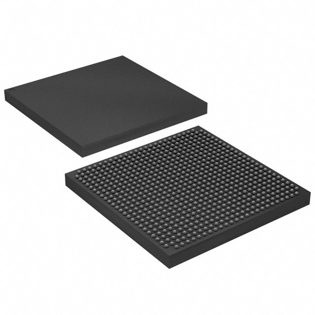
| Package / Case | 1020-BBGA | Number of I/O | 607 | Voltage | 1.425 V - 1.575 V | ||
| Mounting Method | Surface Mount | RoHS Compliance | Unknown | REACH Compliance | REACH Unknown | ||
| Moisture Sensitivity Level | 3 (168 Hours) | Number of LABs/CLBs | 2566 | Number of Logic Elements/Cells | 25660 | ||
| Number of Gates | N/A | ECCN | 3A001A7A | HTS Code | 8542.39.0001 | ||
| Qualification | N/A | Total RAM Bits | 1944576 |
Overview of EP1SGX25DF1020C6N – Stratix® GX Field Programmable Gate Array (FPGA) IC 607 1944576 25660 1020-BBGA
The EP1SGX25DF1020C6N is a commercial-grade Stratix GX family FPGA in a 1020-BBGA package, offering a balance of high logic capacity, on-chip memory, and a large I/O count for complex digital designs. It is a surface-mount device supplied with a core voltage range of 1.425 V to 1.575 V and an operating temperature range of 0 °C to 85 °C.
As a member of the Stratix GX family, this device benefits from the family’s high-speed serial transceiver architecture and scalable logic array, making it suitable for high-speed backplane interfaces, chip-to-chip bridging, and communications protocol applications where integration and performance are required.
Key Features
- Logic Capacity — 25,660 logic elements for implementing complex custom logic and control functions.
- Embedded Memory — Approximately 1.94 Mbits of on-chip RAM to support buffers, FIFOs, and packet processing without reducing logic resources.
- High I/O Count — 607 I/O pins to support dense peripheral, memory, and high-speed interface connections.
- Stratix GX Transceiver Family Features — Family-level transceiver capabilities include clock-data recovery (CDR) and embedded SERDES with data rates up to 3.1875 Gbps, support for common serial protocols, programmable pre-emphasis/equalization, and channel power-down features.
- Advanced FPGA Architecture — Stratix GX family features such as TriMatrix memory organization, high-speed DSP blocks, and multiple PLLs are available within the family architecture to support high-performance signal processing and timing control.
- Package & Mounting — 1020-BBGA package (supplier device package listed as 1020-FBGA, 33 × 33) and surface-mount mounting for space-efficient board designs.
- Power & Thermal — Core voltage supply range of 1.425 V to 1.575 V with a commercial operating temperature range of 0 °C to 85 °C.
- Compliance — RoHS compliant.
Typical Applications
- High‑Speed Backplane Interfaces — Use the device’s family-level serial transceiver capabilities and high I/O count to implement backplane bridging and packet routing.
- Chip‑to‑Chip Interconnect — Leverage embedded SERDES and programmable signal-conditioning features for reliable high-speed links between ICs.
- Communications Protocol Bridging — Implement protocol conversion and protocol-aware packet processing using the FPGA’s logic capacity and on-chip RAM.
- Signal Processing & DSP Acceleration — Use dedicated DSP resources and embedded memory for filtering, accumulation, and other real-time data-path functions.
Unique Advantages
- Substantial Logic Resources: 25,660 logic elements enable implementation of complex custom logic, state machines, and protocol engines within a single device.
- On-Chip Memory for Low-Latency Processing: Approximately 1.94 Mbits of embedded RAM reduce dependence on external memory for buffering and accelerate data-path operations.
- High-Density I/O: 607 I/O pins accommodate multiple parallel buses, memory interfaces, and external peripherals without additional glue logic.
- Family-Level High-Speed Serial Support: Stratix GX transceiver features (up to 3.1875 Gbps) and protocol support simplify integration of high-bandwidth serial links.
- Compact System Integration: 1020-BBGA package and surface-mount mounting enable space-efficient PCB designs for densely populated boards.
- Standards and Environmental Compliance: RoHS compliance aligns with common environmental requirements for commercial electronic products.
Why Choose EP1SGX25DF1020C6N?
The EP1SGX25DF1020C6N delivers a balanced combination of logic density, embedded memory, and extensive I/O in a Stratix GX FPGA package. It is positioned for designers who need scalable FPGA resources alongside the family’s high-speed serial capabilities to implement demanding communications, interfacing, and signal-processing functions.
Choose this device for commercial applications that require integrated on-chip RAM, a high I/O count, and access to the Stratix GX family feature set—providing a pathway to scalable performance within a single, RoHS-compliant FPGA solution.
Request a quote or submit a procurement inquiry to receive pricing and availability for EP1SGX25DF1020C6N.


Date Founded: 1968
Headquarters: Santa Clara, California, USA
Employees: 130,000+
Revenue: $54.23 Billion
Certifications and Memberships: ISO9001:2015, ISO14001:2015, ISO17025:2017, ISO27001:2022, ISO45001:2018, ISO50001:2018


