
EP1SGX40GF1020I6
| Part Description |
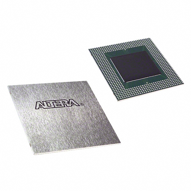
Stratix® GX Field Programmable Gate Array (FPGA) IC 624 3423744 41250 1020-BBGA |
|---|---|
| Quantity | 545 Available (as of June 17, 2026) |

| Product Category | Field Programmable Gate Array (FPGA) |
|---|---|
| Manufacturer | Intel |
| Manufacturing Status | Obsolete |
| Manufacturer Standard Lead Time | Contact Us |
| Datasheet |
Specifications & Environmental
| Device Package | 1020-FBGA (33x33) | Grade | Industrial | Operating Temperature | -40°C – 100°C | ||
|---|---|---|---|---|---|---|---|
| Package / Case | 1020-BBGA | Number of I/O | 624 | Voltage | 1.425 V - 1.575 V | ||
| Mounting Method | Surface Mount | RoHS Compliance | RoHS non-compliant | REACH Compliance | REACH Unknown | ||
| Moisture Sensitivity Level | 3 (168 Hours) | Number of LABs/CLBs | 4125 | Number of Logic Elements/Cells | 41250 | ||
| Number of Gates | N/A | ECCN | 3A001A7A | HTS Code | 8542.39.0001 | ||
| Qualification | N/A | Total RAM Bits | 3423744 |
Overview of EP1SGX40GF1020I6 – Stratix® GX Field Programmable Gate Array (FPGA) IC, 1020‑BBGA
The EP1SGX40GF1020I6 is an Intel Stratix® GX family FPGA offering a scalable, high‑performance 1.5‑V logic array with integrated high‑speed serial transceiver technology. This device targets high‑bandwidth designs with substantial logic capacity, abundant I/O, and embedded memory for applications such as high‑speed backplane interfaces, chip‑to‑chip links, and communications protocol bridging.
Key on‑chip resources include 41,250 logic elements, approximately 3.42 Mbits of embedded memory, and 624 user I/Os packaged in a 1020‑FBGA (33×33) surface‑mount package. The device operates from 1.425 V to 1.575 V and is rated for industrial temperatures (−40 °C to 100 °C).
Key Features
- Core Logic — 41,250 logic elements provide substantial combinational and sequential resources for complex FPGA designs and custom logic implementation.
- Embedded Memory — Approximately 3.42 Mbits of on‑chip RAM, implemented with TriMatrix memory blocks to support true dual‑port memory and FIFO buffers for data buffering and packet storage.
- I/O and Packaging — 624 user I/Os in a 1020‑BBGA / 1020‑FBGA (33×33) surface‑mount package for dense system integration and routing flexibility.
- Voltage and Temperature — Nominal core supply range 1.425 V to 1.575 V; industrial operating range from −40 °C to 100 °C suitable for a wide set of embedded and communications environments.
- High‑Speed Serial Transceivers (Family‑Level) — Stratix GX family transceivers support 500 Mbps to 3.1875 Gbps full‑duplex operation with clock data recovery (CDR), programmable VOD, pre‑emphasis and equalization settings for improved signal integrity.
- Clocking and DSP — Up to eight general‑purpose PLLs, multiple global and regional clock networks, and high‑speed DSP blocks for multiply/accumulate and FIR implementations (as specified for the Stratix GX family).
- Memory & Interfaces Support — Family support for external high‑speed memories and common source‑synchronous bus standards; built‑in features for protocol handling such as 8B/10B encoding/decoding and pattern detection (series‑level capabilities).
- Standards & Design Aids — Series‑level compatibility with common protocols and standards (for example, XAUI and GigE modes) and built‑in test and alignment features to simplify high‑speed link design and validation.
- Regulatory — RoHS compliant.
Typical Applications
- High‑Speed Networking Equipment — Implements packet processing, protocol bridging, and line‑rate interfaces where multi‑Gbps serial links and large logic capacity are required.
- Backplane and Interconnect Systems — Suitable for high‑speed backplane interfaces and chip‑to‑chip links leveraging the Stratix GX transceiver features and abundant I/O.
- Telecommunications and Carrier Systems — Supports protocol adaptation and data buffering with on‑chip RAM and DSP blocks for signal processing tasks.
- High‑Performance Embedded Systems — Acts as a programmable fabric for custom accelerators, interface bridging, and system control in industrial temperature environments.
Unique Advantages
- High Logic Capacity: 41,250 logic elements enable large, complex designs without immediate migration to a higher device family.
- Substantial On‑Chip Memory: Approximately 3.42 Mbits of embedded RAM reduce dependence on external memory for buffering and packet storage, simplifying board design.
- Large I/O Count in a Compact Package: 624 I/Os in a 1020‑FBGA (33×33) package provide routing density for multi‑interface systems while maintaining a compact footprint.
- Industrial Temperature Range: −40 °C to 100 °C rating supports deployment in demanding embedded and communications environments.
- Family‑Level High‑Speed SerDes Features: Stratix GX transceiver capabilities (500 Mbps–3.1875 Gbps) and programmable signal conditioning help meet stringent signal‑integrity and protocol requirements.
- Design Flexibility: On‑chip PLLs, multiple clock networks, and DSP resources support a wide range of application architectures and performance tradeoffs.
Why Choose EP1SGX40GF1020I6?
The EP1SGX40GF1020I6 positions itself as a high‑capacity, flexible FPGA option within the Stratix GX family, combining large logic resources, significant embedded RAM, and a high I/O count in a fine‑pitch FBGA package. Its operating voltage and industrial temperature rating make it suitable for robust embedded and communications applications that require sustained performance across environmental extremes.
Designers seeking a programmable platform with family‑level high‑speed transceiver features, extensive clocking and DSP resources, and RoHS compliance will find this device well suited to prototyping and production deployments where integration and throughput are priorities.
Request a quote or submit a purchase inquiry to begin sourcing EP1SGX40GF1020I6 for your next high‑performance FPGA design.


Date Founded: 1968
Headquarters: Santa Clara, California, USA
Employees: 130,000+
Revenue: $54.23 Billion
Certifications and Memberships: ISO9001:2015, ISO14001:2015, ISO17025:2017, ISO27001:2022, ISO45001:2018, ISO50001:2018


