
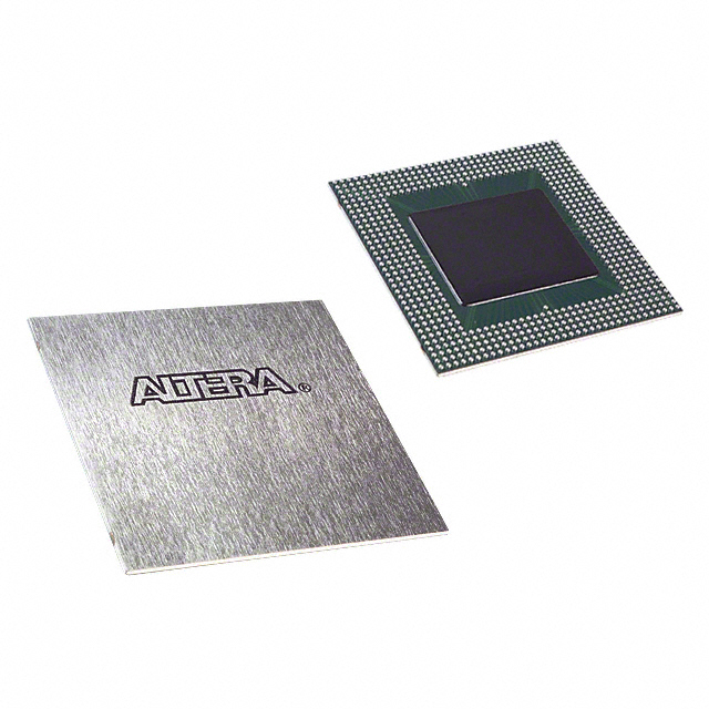
EP20K1000CB652C7
| Part Description |
APEX-20KC® Field Programmable Gate Array (FPGA) IC 488 327680 38400 652-BGA |
|---|---|
| Quantity | 1,005 Available (as of June 15, 2026) |

| Product Category | Field Programmable Gate Array (FPGA) |
|---|---|
| Manufacturer | Intel |
| Manufacturing Status | Obsolete |
| Manufacturer Standard Lead Time | Contact Us |
| Datasheet |
Specifications & Environmental
| Device Package | 652-BGA (45x45) | Grade | Commercial | Operating Temperature | 0°C – 85°C | ||
|---|---|---|---|---|---|---|---|
| Package / Case | 652-BGA | Number of I/O | 488 | Voltage | 1.71 V - 1.89 V | ||
| Mounting Method | Surface Mount | RoHS Compliance | Unknown | REACH Compliance | REACH Unaffected | ||
| Moisture Sensitivity Level | 3 (168 Hours) | Number of LABs/CLBs | 3840 | Number of Logic Elements/Cells | 38400 | ||
| Number of Gates | 1772000 | ECCN | 3A001A2A | HTS Code | 8542.39.0001 | ||
| Qualification | N/A | Total RAM Bits | 327680 |
Overview of EP20K1000CB652C7 – APEX-20KC® Field Programmable Gate Array (FPGA) IC 488 327680 38400 652‑BGA
The EP20K1000CB652C7 is an APEX-20KC family FPGA delivered in a 652‑BGA (45×45) package for surface-mount applications. It integrates a high-density logic fabric with embedded memory and flexible I/O to serve commercial electronic designs that require programmable logic, on‑chip RAM, and extensive I/O connectivity.
This device is built on a copper-metal fabrication process and provides a balance of integration and performance for applications such as high‑speed memory interfaces, system control, and complex bus bridging in commercial products.
Key Features
- Logic Capacity — Up to 38,400 logic elements, enabling implementation of complex custom logic and control functions.
- Gate Density — Up to 1,772,000 system gates (maximum), providing substantial resource headroom for large designs; JTAG boundary-scan circuitry can contribute additional gates.
- Embedded Memory — Approximately 327,680 bits of on-chip RAM for FIFOs, buffers, and temporary storage without reducing available logic.
- I/O Count and Package — 488 user I/Os in a 652‑BGA (45×45) surface-mount package, suitable for designs requiring many external connections.
- Clocking and Timing — Up to four PLLs and support for multiple global clocks to enable flexible clock management and low-skew distribution.
- Process and Performance — Manufactured using a 0.15‑µm all‑layer copper-metal process offering higher performance and lower power compared to previous generations.
- Voltage and Power — Internal supply and core operation centered on 1.8 V; specified supply range 1.71 V to 1.89 V.
- Operating Range — Commercial grade: specified for 0 °C to 85 °C ambient operation.
- Low‑Power and I/O Flexibility — Copper interconnect and MultiVolt I/O support for multiple interface voltage levels, enabling power-optimized designs and mixed-voltage I/O usage.
Typical Applications
- Telecommunications and Networking — Implement protocol handling, packet buffering, and custom data-path logic using the device’s high logic density and on‑chip RAM.
- Memory Interface and Bridge — Support high‑speed external memories and buffer control with embedded RAM and flexible clocking/PLL resources.
- Industrial and Commercial Control Systems — Centralize custom control logic and I/O aggregation for commercial automation, machine control, and instrumentation.
- High‑I/O Embedded Systems — Drive multiple external peripherals and buses with 488 user I/Os in a compact BGA package.
Unique Advantages
- High integration reduces BOM count: Combines tens of thousands of logic elements with substantial on‑chip RAM, minimizing external glue logic and discrete memory needs.
- Flexible clock management: Up to four PLLs and multiple global clocks simplify timing architectures for synchronous designs and high‑speed interfaces.
- Compact, high‑I/O package: 652‑BGA (45×45) package supports 488 user I/Os while keeping board footprint efficient for dense system layouts.
- Commercial temperature qualification: Rated for 0 °C to 85 °C operation, matching the thermal needs of commercial electronic products.
- Manufacturing and power advantages: Copper interconnect process enables improved performance and power characteristics compared to older process generations.
Why Choose EP20K1000CB652C7?
The EP20K1000CB652C7 positions itself as a versatile, high‑density FPGA for commercial applications that demand substantial logic resources, embedded memory, and a large I/O complement in a compact BGA package. Its architecture and clocking resources make it suitable for designs involving high‑speed interfaces, complex control logic, and significant on‑chip buffering.
For design teams needing a programmable platform with defined electrical and thermal characteristics—1.71–1.89 V supply range and 0 °C to 85 °C operation—this device offers a verified option with substantial logic and RAM capacity and multiple PLLs for timing flexibility.
Request a quote or submit a purchase inquiry to evaluate EP20K1000CB652C7 for your next commercial FPGA design project.


Date Founded: 1968
Headquarters: Santa Clara, California, USA
Employees: 130,000+
Revenue: $54.23 Billion
Certifications and Memberships: ISO9001:2015, ISO14001:2015, ISO17025:2017, ISO27001:2022, ISO45001:2018, ISO50001:2018


