
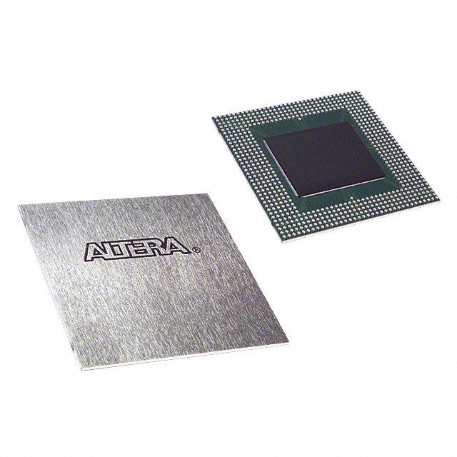
EP20K1000CB652C8ES
| Part Description |
APEX-20KC® Field Programmable Gate Array (FPGA) IC 488 327680 38400 652-BGA |
|---|---|
| Quantity | 154 Available (as of June 15, 2026) |

| Product Category | Field Programmable Gate Array (FPGA) |
|---|---|
| Manufacturer | Intel |
| Manufacturing Status | Obsolete |
| Manufacturer Standard Lead Time | Contact Us |
| Datasheet |
Specifications & Environmental
| Device Package | 652-BGA (45x45) | Grade | Commercial | Operating Temperature | 0°C – 85°C | ||
|---|---|---|---|---|---|---|---|
| Package / Case | 652-BGA | Number of I/O | 488 | Voltage | 1.71 V - 1.89 V | ||
| Mounting Method | Surface Mount | RoHS Compliance | Unknown | REACH Compliance | REACH Unknown | ||
| Moisture Sensitivity Level | 3 (168 Hours) | Number of LABs/CLBs | 3840 | Number of Logic Elements/Cells | 38400 | ||
| Number of Gates | 1772000 | ECCN | OBSOLETE | HTS Code | 0000.00.0000 | ||
| Qualification | N/A | Total RAM Bits | 327680 |
Overview of EP20K1000CB652C8ES – APEX-20KC® Field Programmable Gate Array (FPGA) IC 488 327680 38400 652-BGA
The EP20K1000CB652C8ES is an APEX-20KC family field programmable gate array (FPGA) offering a high-density MultiCore architecture that integrates look-up table (LUT) logic with embedded memory blocks. It provides 38,400 logic elements and approximately 0.328 Mbits of embedded RAM to support complex programmable logic and memory-centric functions.
Designed for applications requiring abundant I/O and flexible clocking, this device delivers up to 488 user I/O pins, a 652-BGA (45×45) package, and low-voltage operation with an internal supply around 1.8 V (specified supply range 1.71 V to 1.89 V). The commercial-grade part supports operation from 0 °C to 85 °C.
Key Features
- Programmable Logic Core 38,400 logic elements and up to 1,772,000 system gates for high-density logic integration.
- Embedded Memory Approximately 327,680 RAM bits available as embedded system blocks (ESBs) for FIFOs, dual-port RAM, and CAM implementations.
- MultiCore Architecture Integrated LUT logic and embedded memory for register-intensive and memory functions without reducing available logic.
- Advanced Process and Interconnect Manufactured on a 0.15‑µm all-layer copper-metal process with a four-level FastTrack® interconnect structure for predictable, high-performance routing.
- Flexible Clocking Up to four phase-locked loops (PLLs) with features including ClockLock, ClockBoost, and ClockShift for phase, multiplication/division, and skew control.
- High-Performance I/O 488 user I/O pins with MultiVolt I/O support (1.8 V, 2.5 V, 3.3 V) and support for advanced standards including LVDS (16 input and 16 output LVDS channels at 840 Mbps).
- Memory and Bus Support Designed to interface with high-speed external memories (DDR SDRAM, ZBT SRAM) and compatible with PCI 2.2 signaling for 3.3-V operation.
- Low-Power Design 1.8-V internal supply and copper interconnects reduce power consumption; ESBs include programmable power-saving modes.
- Dedicated Arithmetic and Cascade Chains Built-in carry and cascade chains accelerate adders, counters, and high-fan-in logic without manual routing.
- Package and Thermal 652‑BGA (45×45) surface-mount package; commercial operating range 0 °C to 85 °C.
Typical Applications
- Networking and Telecom High I/O count, LVDS channels, and memory interface support make this device suitable for packet processing, line cards, and protocol bridging.
- Memory and Storage Interfaces Direct support for DDR SDRAM and ZBT SRAM enables implementation of high-speed memory controllers and buffering logic.
- Custom Hardware Acceleration Large logic capacity and dedicated arithmetic chains enable hardware acceleration for signal processing and algorithm offload.
- PCI-Based Systems PCI 2.2 compliant signaling for 3.3‑V operation supports bridging and I/O expansion in host-based systems.
Unique Advantages
- Highly integrated logic and memory: Combines 38,400 logic elements with ~0.328 Mbits of embedded RAM to consolidate functions and reduce external components.
- Flexible multi-voltage I/O: MultiVolt I/O support (1.8 V, 2.5 V, 3.3 V) simplifies interfacing to a wide range of peripherals and memory devices.
- Robust clock management: Up to four PLLs and advanced clock features provide control over phase, skew, and frequency for timing-critical systems.
- High channel density: 488 user I/Os and dedicated LVDS channels support complex multi-channel designs and high-speed serial interfaces.
- Performance-oriented fabrication: 0.15‑µm copper-metal process and FastTrack interconnects deliver predictable routing and reduced power.
- Package and I/O scalability: 652‑BGA (45×45) package supports high pin-count designs while maintaining surface-mount compatibility.
Why Choose EP20K1000CB652C8ES?
The EP20K1000CB652C8ES positions itself as a high-density, flexible FPGA platform for designs that require substantial logic capacity, embedded memory, and a large I/O footprint. Its MultiCore architecture, advanced clocking, and memory interfacing capabilities make it suitable for complex system functions such as protocol handling, memory controllers, and hardware acceleration.
For engineering teams and procurement looking for a commercially graded FPGA with strong integration, predictable interconnect, and multi-voltage I/O support, this device provides a balanced combination of performance, power-conscious design, and interface versatility backed by the APEX-20KC family feature set.
Request a quote or submit an inquiry to learn more about availability and pricing for EP20K1000CB652C8ES. Our team can assist with technical details, lead times, and order submission.


Date Founded: 1968
Headquarters: Santa Clara, California, USA
Employees: 130,000+
Revenue: $54.23 Billion
Certifications and Memberships: ISO9001:2015, ISO14001:2015, ISO17025:2017, ISO27001:2022, ISO45001:2018, ISO50001:2018


