
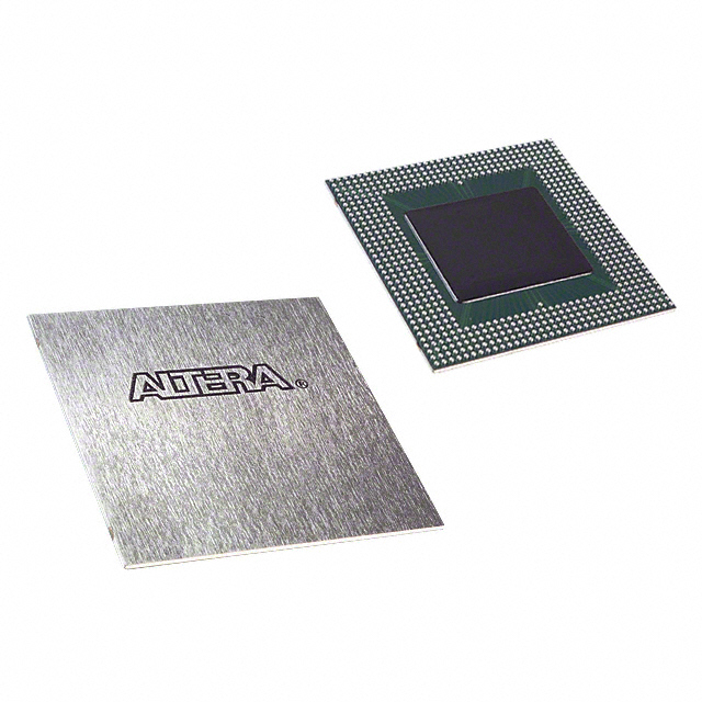
EP20K1000CB652C9N
| Part Description |
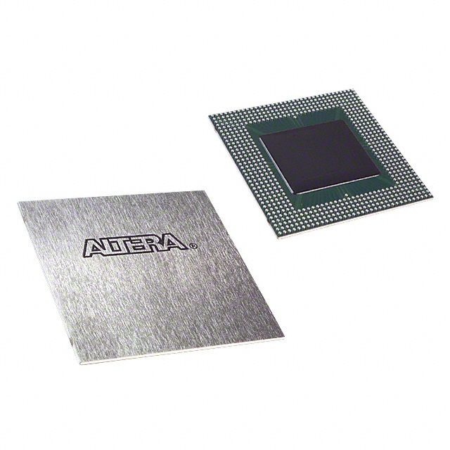
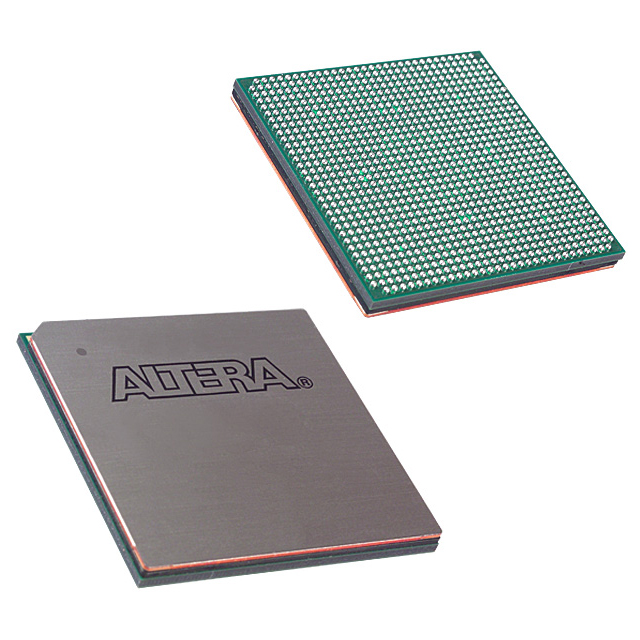
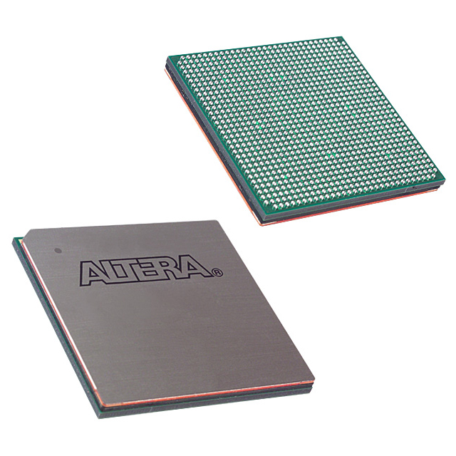
APEX-20KC® Field Programmable Gate Array (FPGA) IC 488 327680 38400 652-BGA |
|---|---|
| Quantity | 305 Available (as of October 7, 2026) |
| Product Category | Field Programmable Gate Array (FPGA) |
|---|---|
| Manufacturer | Intel |
| Manufacturing Status | Active |
| Manufacturer Standard Lead Time | 14 Weeks |
| Datasheet |
Specifications & Environmental
| Device Package | 652-BGA (45x45) | Grade | Commercial | Operating Temperature | 0°C – 85°C | ||
|---|---|---|---|---|---|---|---|
| Package / Case | 652-BGA | Number of I/O | 488 | Voltage | 1.71 V - 1.89 V | ||
| Mounting Method | Surface Mount | RoHS Compliance | RoHS Compliant | REACH Compliance | REACH Unaffected | ||
| Moisture Sensitivity Level | 3 (168 Hours) | Number of LABs/CLBs | 3840 | Number of Logic Elements/Cells | 38400 | ||
| Number of Gates | 1772000 | ECCN | PENDING ECCN | HTS Code | 0000.00.0000 | ||
| Qualification | N/A | Total RAM Bits | 327680 |
Overview of EP20K1000CB652C9N – APEX-20KC FPGA, 652-BGA, 38,400 logic elements
The EP20K1000CB652C9N is an APEX-20KC family field programmable gate array (FPGA) packaged in a 652-ball BGA (45×45) intended for commercial applications. It combines a MultiCore architecture with look-up table (LUT) logic and embedded memory to deliver high-density programmable logic suitable for designs that require significant on-chip RAM, flexible I/O, and multiple clock-management resources.
With 38,400 logic elements, approximately 0.328 Mbits of embedded memory, up to four PLLs, and support for high-speed external memories and I/O standards, this device targets applications needing dense logic, memory buffering, and complex interface support while operating from a 1.71 V–1.89 V internal supply.
Key Features
- Core architecture MultiCore architecture integrating LUT-based logic and embedded system blocks (ESBs) for efficient implementation of register‑intensive functions and memory functions such as FIFOs and dual-port RAM.
- Logic capacity 38,400 logic elements and up to 1,772,000 gates (maximum system gates) provide high-density programmable resources for complex logic designs.
- Embedded memory Approximately 0.328 Mbits (327,680 total RAM bits) of on-chip RAM available without reducing logic capacity, plus 160 ESBs for memory-oriented functions.
- Clock and timing Up to four phase-locked loops (PLLs), a built-in low-skew clock tree, and support for up to eight global clock signals enable flexible clock management and phase/delay control.
- I/O and interface support 488 user I/O pins, MultiVolt I/O support (1.8 V, 2.5 V, 3.3 V), and documented support for interfaces including PCI Local Bus operation, DDR SDRAM, ZBT SRAM, and LVDS channels (16 inputs and 16 outputs at 840 Mbps).
- Low-power design 1.8 V internal supply (device operates within 1.71 V–1.89 V range) and copper interconnect technology described for reduced power consumption; ESBs include programmable power-saving modes.
- Package and operating range Surface-mount 652-BGA (45×45) package; commercial grade with an operating temperature range of 0 °C to 85 °C.
- Design tools and IP Supported by the Quartus II development system and Altera MegaCore functions and AMPP megafunctions optimized for the APEX 20KC architecture.
Typical Applications
- High-speed interface bridging Implement PCI‑based interfaces, DDR SDRAM controllers, and LVDS channel adapters where dense logic and flexible I/O are required.
- Memory buffering and traffic management Use embedded RAM and ESBs to build FIFOs, dual-port RAM blocks, and buffering logic for data stream and packet handling.
- Complex control and signal-processing glue logic Deploy the device for protocol translation, custom datapath logic, and control-state machines that benefit from dedicated carry and cascade chains.
- Prototyping and system integration Leverage the device’s high logic density and rich I/O set for prototyping feature-rich embedded systems and integration of multiple peripheral buses.
Unique Advantages
- High-density programmable fabric: 38,400 logic elements and up to 1.77 million gates enable consolidation of multiple functions into a single device.
- Significant embedded memory: Approximately 0.328 Mbits of RAM and 160 ESBs allow on-chip storage for buffering and memory-mapped logic without consuming additional logic elements.
- Flexible I/O standards: MultiVolt I/O and documented support for PCI, DDR SDRAM, ZBT SRAM, and LVDS provide integration options for modern system interfaces.
- Comprehensive clock management: Up to four PLLs and multiple global clocks simplify timing architectures for multi-domain designs.
- Toolchain and IP support: Compatibility with the Quartus II development system and available MegaCore megafunctions accelerates development and integration.
- Commercial-grade packaging: 652‑BGA surface-mount package (45×45) suited to production assemblies within a 0 °C–85 °C operating range.
Why Choose EP20K1000CB652C9N?
The EP20K1000CB652C9N positions itself as a high-density, feature-rich FPGA for commercial applications that require substantial logic capacity, embedded memory, and flexible interface support. Its MultiCore architecture, multiple PLLs, and extensive I/O options make it appropriate for designs integrating memory controllers, high-speed interfaces, and complex control logic.
Backed by the Quartus II development environment and optimized MegaCore functions, this device offers a clear path for development, IP integration, and system-level consolidation—delivering scalability and deployment-ready capabilities for projects that demand significant programmable resources within a commercial operating range.
If you would like pricing, lead-time information, or to submit a quote request for EP20K1000CB652C9N, please request a quote or contact our sales team to initiate a purchase inquiry.





















Date Founded: 1968
Headquarters: Santa Clara, California, USA
Employees: 130,000+
Revenue: $54.23 Billion
Certifications and Memberships: ISO9001:2015, ISO14001:2015, ISO17025:2017, ISO27001:2022, ISO45001:2018, ISO50001:2018


