
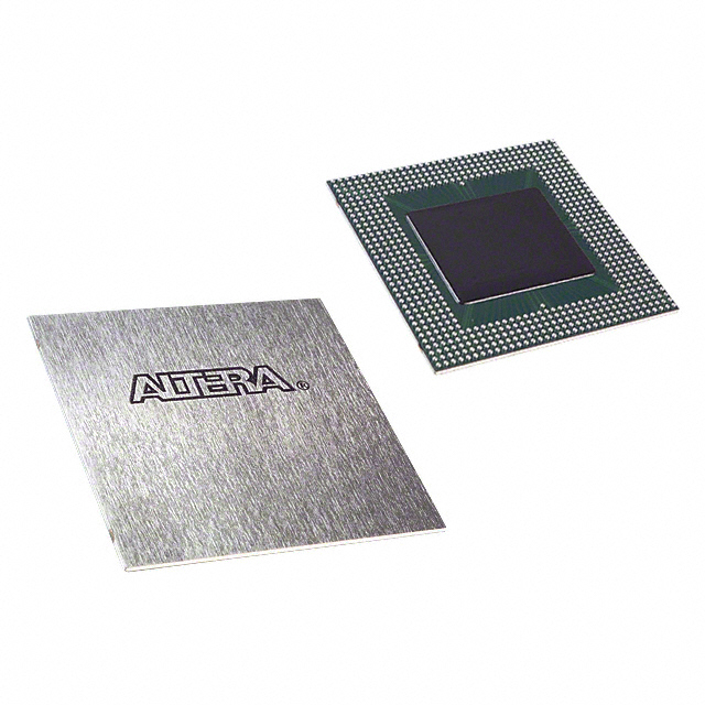
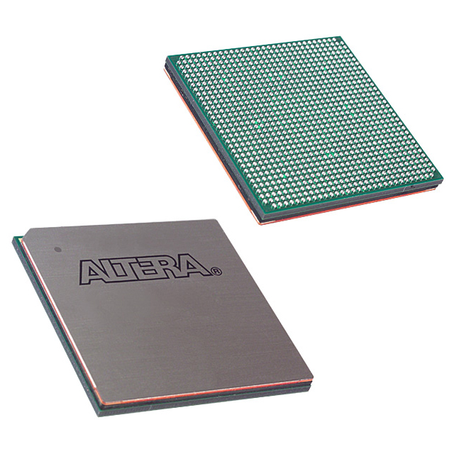
EP20K1000CF33C7N
| Part Description |
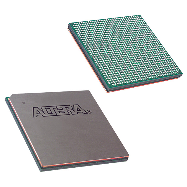
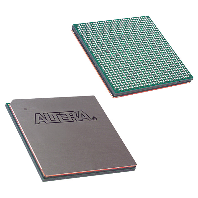
APEX-20KC® Field Programmable Gate Array (FPGA) IC 708 327680 38400 1020-BBGA |
|---|---|
| Quantity | 1,130 Available (as of October 8, 2026) |
| Product Category | Field Programmable Gate Array (FPGA) |
|---|---|
| Manufacturer | Intel |
| Manufacturing Status | Active |
| Manufacturer Standard Lead Time | 14 Weeks |
| Datasheet |
Specifications & Environmental
| Device Package | 1020-FBGA (33x33) | Grade | Commercial | Operating Temperature | 0°C – 85°C | ||
|---|---|---|---|---|---|---|---|
| Package / Case | 1020-BBGA | Number of I/O | 708 | Voltage | 1.71 V - 1.89 V | ||
| Mounting Method | Surface Mount | RoHS Compliance | RoHS Compliant | REACH Compliance | REACH Unaffected | ||
| Moisture Sensitivity Level | 3 (168 Hours) | Number of LABs/CLBs | 3840 | Number of Logic Elements/Cells | 38400 | ||
| Number of Gates | 1772000 | ECCN | PENDING ECCN | HTS Code | 0000.00.0000 | ||
| Qualification | N/A | Total RAM Bits | 327680 |
Overview of EP20K1000CF33C7N – APEX-20KC® Field Programmable Gate Array (FPGA) IC 708 327680 38400 1020-BBGA
The EP20K1000CF33C7N is an APEX-20KC series programmable logic device (PLD) offering MultiCore architecture combining look-up table logic and embedded memory. With 38,400 logic elements and approximately 0.328 Mbits of embedded RAM (327,680 bits), this device targets applications that require a high degree of on-chip logic and memory integration.
Designed for commercial-grade systems, the device provides up to 708 user I/O pins in a 1020-ball BGA package and operates from a primary internal supply around 1.8 V (specified supply range 1.71 V to 1.89 V). It supports features aimed at performance, flexible I/O, and low-power operation as documented in the APEX 20KC family datasheet.
Key Features
- Core Logic — 38,400 logic elements (LEs) and up to 1,772,000 system gates, enabling complex programmable logic implementations.
- On‑Chip Memory — Approximately 0.328 Mbits of embedded RAM (327,680 bits) and 160 embedded system blocks (ESBs) for FIFOs, dual-port RAM, and CAM functions.
- I/O and Interfaces — Up to 708 user I/O pins with MultiVolt I/O support for 1.8 V, 2.5 V, and 3.3 V interfaces; support for a range of advanced I/O standards and hot-socketing operation as described in the datasheet.
- Clock and Timing — Flexible clock management including up to four phase‑locked loops (PLLs), up to eight global clock signals, and built‑in low‑skew clock tree features such as ClockLock and ClockBoost.
- High‑Performance Interconnect — Copper interconnect with a four‑level hierarchical FastTrack interconnect structure, dedicated carry and cascade chains, and interleaved local interconnect for low-latency routing.
- Power and Voltage — Low‑power design with 1.8 V internal supply (VCCINT) and copper interconnect to reduce power; device-level supply range specified at 1.71 V to 1.89 V. ESBs include programmable power‑saving modes.
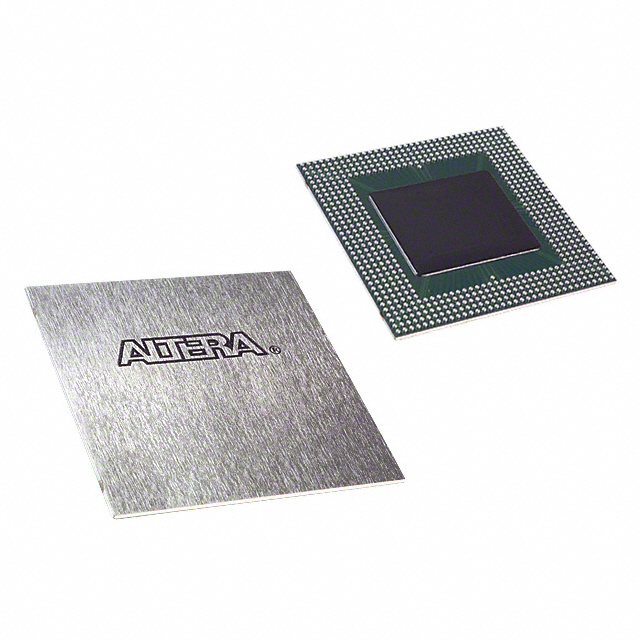
- Package and Mounting — 1020‑BBGA package (supplier package: 1020‑FBGA, 33 × 33) for surface-mount assembly; RoHS compliant and rated for commercial operating temperatures.
- Operating Range — Commercial temperature grade with an operating range of 0 °C to 85 °C.
Typical Applications
- High‑performance embedded logic — Implement custom datapaths, control logic, and state machines using the device's large LE count and dedicated carry/cascade chains.
- Memory interface and buffering — Use embedded system blocks for FIFOs and dual‑port RAM to support DDR/SDRAM and ZBT SRAM interfaces and buffering tasks.
- High‑speed I/O and communications — Leverage MultiVolt I/O support and LVDS capability for multi‑standard interface bridging and high‑throughput links.
- Prototyping and system integration — Combine significant on‑chip logic and memory to consolidate functions and reduce external component count in prototype and production boards.
Unique Advantages
- High logic and memory integration: 38,400 logic elements and approximately 0.328 Mbits of embedded RAM reduce the need for external components and simplify board-level design.
- Flexible I/O voltage support: MultiVolt I/O for 1.8 V, 2.5 V, and 3.3 V interfaces enables direct interfacing to a variety of external devices and standards.
- Advanced clock management: Up to four PLLs and up to eight global clocks provide the timing resources needed for multi‑domain systems and frequency synthesis.
- Deterministic, low‑latency routing: Four‑level FastTrack interconnect, dedicated carry and cascade chains, and interleaved local interconnect support predictable timing and fast logic paths.
- Commercial temperature and RoHS compliance: Surface‑mount 1020‑BBGA package rated for 0 °C to 85 °C operation and RoHS‑compliant construction for mainstream electronic products.
Why Choose EP20K1000CF33C7N?
EP20K1000CF33C7N positions itself as a high‑capacity APEX‑20KC FPGA optimized for designs that require substantial on‑chip logic and embedded memory combined with broad I/O connectivity. Its MultiCore architecture, copper interconnect, and integrated clock management give designers the building blocks to implement complex, timing‑sensitive systems while reducing external component count.
This device is suitable for commercial applications that benefit from integrated memory blocks, a large number of I/Os, and flexible voltage interfacing. It delivers a balance of performance, integration, and power-conscious design for customers developing advanced logic, memory interfacing, and high‑speed I/O solutions.
Request a quote or submit an inquiry to get pricing and availability for EP20K1000CF33C7N and to discuss how this APEX‑20KC device can fit your design requirements.





















Date Founded: 1968
Headquarters: Santa Clara, California, USA
Employees: 130,000+
Revenue: $54.23 Billion
Certifications and Memberships: ISO9001:2015, ISO14001:2015, ISO17025:2017, ISO27001:2022, ISO45001:2018, ISO50001:2018


