
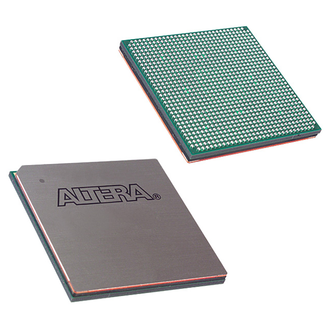
EP20K1000CF33C8ES
| Part Description |
APEX-20KC® Field Programmable Gate Array (FPGA) IC 708 327680 38400 1020-BBGA |
|---|---|
| Quantity | 199 Available (as of June 16, 2026) |

| Product Category | Field Programmable Gate Array (FPGA) |
|---|---|
| Manufacturer | Intel |
| Manufacturing Status | Obsolete |
| Manufacturer Standard Lead Time | Contact Us |
| Datasheet |
Specifications & Environmental
| Device Package | 1020-FBGA (33x33) | Grade | Commercial | Operating Temperature | 0°C – 85°C | ||
|---|---|---|---|---|---|---|---|
| Package / Case | 1020-BBGA | Number of I/O | 708 | Voltage | 1.71 V - 1.89 V | ||
| Mounting Method | Surface Mount | RoHS Compliance | Unknown | REACH Compliance | REACH Unknown | ||
| Moisture Sensitivity Level | 3 (168 Hours) | Number of LABs/CLBs | 3840 | Number of Logic Elements/Cells | 38400 | ||
| Number of Gates | 1772000 | ECCN | OBSOLETE | HTS Code | 0000.00.0000 | ||
| Qualification | N/A | Total RAM Bits | 327680 |
Overview of EP20K1000CF33C8ES – APEX-20KC Field Programmable Gate Array, 38,400 LEs, 327,680-bit RAM, 708 I/O, 1020-BBGA
The EP20K1000CF33C8ES is an APEX-20KC series Field Programmable Gate Array (FPGA) IC designed for commercial-grade embedded and system applications. It implements a MultiCore architecture combining look-up table (LUT) logic and embedded system blocks (ESBs) to deliver flexible logic and on-chip memory for control, interface, and buffering functions.
With 38,400 logic elements, approximately 327,680 bits of embedded memory, and up to 708 user I/O pins in a 1020-BBGA (33×33) package, this device targets designs that require high I/O density, integrated memory, and configurable clock management while operating within a 0 °C to 85 °C commercial range.
Key Features
- Core Architecture MultiCore architecture that integrates LUT-based logic and embedded system blocks (ESBs) for register-intensive functions and memory implementation such as FIFOs and dual-port RAM.
- Logic Density 38,400 logic elements with a maximum of 1,772,000 system gates, providing substantial programmable logic capacity for complex designs.
- Embedded Memory Approximately 0.33 Mbits (327,680 bits) of on-chip RAM available without reducing logic capacity, suitable for buffering and local storage.
- I/O and Interface Support Up to 708 user I/O pins with MultiVolt I/O support (1.8 V, 2.5 V, 3.3 V and 5.0 V via external resistor as noted in the series datasheet) and dedicated support for high-speed differential interfaces such as LVDS channels.
- Clock Management Up to four phase-locked loops (PLLs) with built-in low-skew clock tree and features for clock phase, delay shifting, and clock multiplication/division.
- Process and Power Manufactured on a 0.15 μm all-layer copper-metal process for improved interconnect performance and lower power; internal supply voltage centered at 1.8 V (specified supply range 1.71 V to 1.89 V in product data).
- Package & Mounting Surface-mount 1020-BBGA package (33×33) suitable for board-level integration where high I/O density is required.
- Commercial Grade & Environmental Commercial grade device with an operating range of 0 °C to 85 °C and RoHS compliance for environmental compatibility.
Typical Applications
- Memory Interface Controllers Use the integrated memory and interface architecture for DDR SDRAM and ZBT SRAM controller implementations and high-speed buffering.
- System Interface and Bridging Leverage MultiVolt I/O and PCI-compliant signaling capabilities for PCI/PCI-X/AGP bridging, bus interfacing, and protocol conversion.
- High-speed Data I/O Deploy LVDS channels and high-density I/O for multi-channel data acquisition, serialization/deserialization, and high-throughput communications links.
- Embedded Control and Processing Implement custom control logic, FIFOs, and dual-port RAM using ESBs and LUT logic for real-time packet or signal processing tasks.
Unique Advantages
- Highly integrated logic and memory: Combines 38,400 logic elements with approximately 0.33 Mbits of embedded RAM to reduce external memory requirements and simplify board design.
- High I/O density: Up to 708 user I/O pins in a 1020-BBGA package enables dense connectivity for multi-channel and multi-interface systems.
- Flexible clocking: Up to four PLLs and dedicated clock features (phase/delay shifting, multiplication/division) enable precise timing control for complex, multi-domain designs.
- Performance-focused process: 0.15 μm copper-metal fabrication delivers improved interconnect performance and reduced power compared to previous APEX generations (series-level detail).
- Commercial-ready and RoHS compliant: Designed for 0 °C to 85 °C operation with RoHS compliance to meet common commercial and environmental requirements.
- Surface-mount, board-friendly package: 1020-BBGA (33×33) package supports high-density PCB layouts and modern surface-mount assembly flows.
Why Choose EP20K1000CF33C8ES?
The EP20K1000CF33C8ES delivers a balance of programmable logic capacity, embedded memory, and broad I/O support in a single commercial-grade FPGA. Its MultiCore architecture and ESBs provide designers with flexible resources for implementing register-intensive functions, memory buffers, and interface logic without sacrificing available logic elements.
This device is well-suited for system designers who need high I/O count, integrated memory for buffering, and configurable clock management within standard commercial temperature and supply ranges. The combination of on-chip resources and package density helps reduce BOM complexity and supports scalable designs backed by the APEX-20KC series documentation and toolchain support.
Request a quote or submit an inquiry to receive pricing and availability information for EP20K1000CF33C8ES and to discuss how this FPGA can meet your design requirements.


Date Founded: 1968
Headquarters: Santa Clara, California, USA
Employees: 130,000+
Revenue: $54.23 Billion
Certifications and Memberships: ISO9001:2015, ISO14001:2015, ISO17025:2017, ISO27001:2022, ISO45001:2018, ISO50001:2018


