
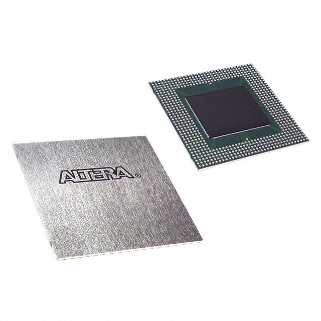
EP20K1000CF33C7
| Part Description |
APEX-20KC® Field Programmable Gate Array (FPGA) IC 708 327680 38400 1020-BBGA |
|---|---|
| Quantity | 648 Available (as of June 15, 2026) |

| Product Category | Field Programmable Gate Array (FPGA) |
|---|---|
| Manufacturer | Intel |
| Manufacturing Status | Obsolete |
| Manufacturer Standard Lead Time | Contact Us |
| Datasheet |
Specifications & Environmental
| Device Package | 1020-FBGA (33x33) | Grade | Commercial | Operating Temperature | 0°C – 85°C | ||
|---|---|---|---|---|---|---|---|
| Package / Case | 1020-BBGA | Number of I/O | 708 | Voltage | 1.71 V - 1.89 V | ||
| Mounting Method | Surface Mount | RoHS Compliance | Unknown | REACH Compliance | REACH Unaffected | ||
| Moisture Sensitivity Level | 3 (168 Hours) | Number of LABs/CLBs | 3840 | Number of Logic Elements/Cells | 38400 | ||
| Number of Gates | 1772000 | ECCN | 3A001A2A | HTS Code | 8542.39.0001 | ||
| Qualification | N/A | Total RAM Bits | 327680 |
Overview of EP20K1000CF33C7 – APEX-20KC FPGA · 38,400 logic elements · 327,680 RAM bits · 708 I/O · 1020-BBGA
The EP20K1000CF33C7 is an APEX-20KC series field programmable gate array (FPGA) IC offering a high-density, low-power programmable logic solution. It integrates a MultiCore architecture with look-up table (LUT) logic and embedded memory blocks to address designs requiring significant logic capacity and on-chip RAM.
Targeted at applications that demand flexible system integration, this commercial-grade device delivers up to 1,772,000 system gates, approximately 0.328 Mbits of embedded memory, and 708 user I/O pins in a 1020-BBGA (33×33) package while operating over a 1.71–1.89 V internal supply and a 0 °C to 85 °C temperature range.
Key Features
- Core Architecture — MultiCore architecture combining LUT-based logic and embedded memory for register-intensive and memory-intensive functions.
- Logic Capacity — 38,400 logic elements (LEs) and a maximum of 1,772,000 system gates provide high-density programmable logic resources.
- Embedded Memory — Approximately 0.328 Mbits (327,680 bits) of on-chip RAM and multiple embedded system blocks (ESBs) usable for FIFO, dual-port RAM, and CAM implementations.
- I/O and Package — 708 user I/O pins in a 1020-BBGA (33×33) package, supporting a wide range of external interfaces and high pin count designs.
- Power and Supply — Internal supply operating in the 1.71 V to 1.89 V range; copper interconnect and low-power design techniques to reduce power consumption.
- Clock Management — Flexible clocking with up to four PLLs, built-in low-skew clock tree, and multiple global clock signals for synchronized system timing.
- High-Speed I/O Features — Support for advanced I/O standards and high-speed memory interfaces; LVDS channels and direct I/O-to-local-interconnect paths for improved timing.
- Operating Range & Compliance — Commercial grade device rated for 0 °C to 85 °C and RoHS compliant.
- Software Ecosystem — Supported by Altera Quartus II development software and Altera MegaCore® functions for synthesis, place-and-route, and optimized megafunctions.
Typical Applications
- System Integration & Glue Logic — Implement complex glue logic and bus bridging with abundant logic elements and a high I/O count for board-level interfacing.
- Memory Interface Control — Support for DDR SDRAM and ZBT SRAM interfaces enables on-board memory controllers and buffering using embedded system blocks.
- High-Speed Serial and Differential I/O — LVDS-capable channels and programmable I/O features make the device suitable for high-speed data links and sensor interfaces.
- Custom Processing and Acceleration — Use the device’s large LUT fabric and embedded RAM for custom datapaths, FIFOs, and on-chip acceleration of compute kernels.
Unique Advantages
- High Logic Density: 38,400 LEs and up to 1,772,000 system gates enable integration of complex logic and state machines on a single device, reducing system BOM.
- Substantial On-Chip Memory: Approximately 0.328 Mbits of embedded RAM and ESBs support deep FIFOs, dual-port RAM, and CAM functions without sacrificing logic capacity.
- Flexible Clocking: Up to four PLLs and an integrated low-skew clock tree simplify multi-clock-domain designs and timing management.
- Wide I/O Capability: 708 user I/O pins and MultiVolt I/O support provide interface flexibility for 1.8 V, 2.5 V, and 3.3 V signaling environments (as supported by the APEX 20KC series).
- Low-Power Copper Interconnect: Copper interconnect and device-level power features reduce power consumption for dense designs.
- Established Tool Support: Quartus II and Altera MegaCore functions provide a mature development flow, easing synthesis, place-and-route, and IP integration.
Why Choose EP20K1000CF33C7?
The EP20K1000CF33C7 positions itself as a high-density, commercially graded FPGA within the APEX-20KC family, combining substantial logic capacity, embedded memory, and a large I/O complement in a 1020-BBGA package. Its MultiCore architecture, clock management features, and low-power copper interconnect make it suited to designs that require integration of complex logic, memory buffering, and high-speed interfaces.
This device is appropriate for engineering teams and designers seeking a configurable, well-supported FPGA platform for mid-to-high complexity applications where performance, integration, and established development tooling are key considerations.
Request a quote or contact our sales team to discuss pricing, availability, and how EP20K1000CF33C7 can be integrated into your next design.


Date Founded: 1968
Headquarters: Santa Clara, California, USA
Employees: 130,000+
Revenue: $54.23 Billion
Certifications and Memberships: ISO9001:2015, ISO14001:2015, ISO17025:2017, ISO27001:2022, ISO45001:2018, ISO50001:2018


