
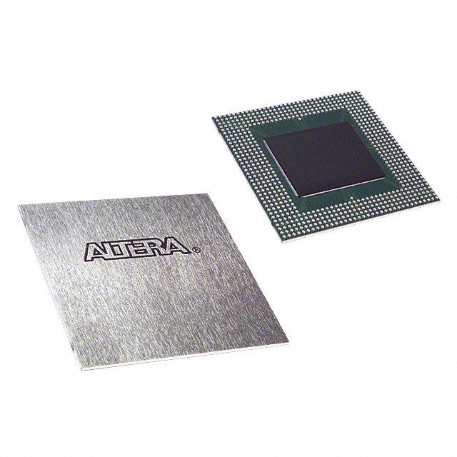
EP20K1000CB652C8
| Part Description |
APEX-20KC® Field Programmable Gate Array (FPGA) IC 488 327680 38400 652-BGA |
|---|---|
| Quantity | 195 Available (as of June 14, 2026) |

| Product Category | Field Programmable Gate Array (FPGA) |
|---|---|
| Manufacturer | Intel |
| Manufacturing Status | Obsolete |
| Manufacturer Standard Lead Time | Contact Us |
| Datasheet |
Specifications & Environmental
| Device Package | 652-BGA (45x45) | Grade | Commercial | Operating Temperature | 0°C – 85°C | ||
|---|---|---|---|---|---|---|---|
| Package / Case | 652-BGA | Number of I/O | 488 | Voltage | 1.71 V - 1.89 V | ||
| Mounting Method | Surface Mount | RoHS Compliance | Unknown | REACH Compliance | REACH Unaffected | ||
| Moisture Sensitivity Level | 3 (168 Hours) | Number of LABs/CLBs | 3840 | Number of Logic Elements/Cells | 38400 | ||
| Number of Gates | 1772000 | ECCN | 3A001A2A | HTS Code | 8542.39.0001 | ||
| Qualification | N/A | Total RAM Bits | 327680 |
Overview of EP20K1000CB652C8 – APEX-20KC® Field Programmable Gate Array (FPGA) IC 488 327680 38400 652-BGA
The EP20K1000CB652C8 is a high-density APEX-20KC series Field Programmable Gate Array (FPGA) in a 652-ball BGA package. It integrates a MultiCore architecture with LUT-based logic and embedded memory blocks to support register-intensive logic and on-chip memory functions.
Designed for commercial-grade applications, this device targets systems that require large logic capacity, substantial embedded RAM, and abundant I/O for high‑speed interfaces and memory subsystems.
Key Features
- Core Logic Up to 38,400 logic elements and approximately 1,772,000 system gates for high-density logic integration.
- Embedded Memory Approximately 0.33 Mbits of embedded memory (327,680 bits) implemented as Embedded System Blocks (ESBs) for FIFOs, dual-port RAM, and CAM-like functions.
- I/O Density and Standards 488 user I/O pins with MultiVolt I/O support for 1.8 V, 2.5 V, and 3.3 V interfaces and support for a wide range of advanced I/O signaling options.
- Clock Management Up to four PLLs with a built-in low-skew clock tree, up to eight global clock signals, and features for phase/delay adjustment and clock multiplication/division.
- Advanced Interconnect Copper interconnect with a four-level FastTrack® hierarchical interconnect structure, dedicated carry and cascade chains, and interleaved local interconnect for predictable, fast routing.
- Power and Supply Core voltage supply specified at 1.71 V to 1.89 V (internal supply VCCINT 1.8 V). ESBs include programmable power-saving modes.
- Package and Mounting 652‑BGA (45 × 45 mm) surface-mount package suitable for compact board designs.
- Operating Range and Grade Commercial grade with an operating temperature range of 0 °C to 85 °C.
- Standards & Interfaces Built-in support for high-speed memory interfaces (including DDR SDRAM and ZBT SRAM), PCI 3.3 V operation per PCI Local Bus Specification Rev. 2.2, and LVDS channels for high-speed serial signaling.
- Compliance RoHS compliant.
Typical Applications
- High‑performance embedded systems — Large logic capacity and integrated memory make this FPGA suitable for control and processing tasks where on-chip resources reduce external component count.
- Memory interface controllers — Native support for DDR SDRAM and ZBT SRAM interfaces and ESBs for FIFO implementation simplify buffering and memory arbitration designs.
- High‑speed I/O and bridging — 488 user I/Os, LVDS channel support, and MultiVolt I/O enable protocol bridging and high-speed data paths between heterogeneous subsystems.
- Custom logic and signal processing — Dedicated carry and cascade chains accelerate arithmetic and wide combinatorial functions commonly used in DSP and control logic.
Unique Advantages
- High logic density: 38,400 logic elements and approximately 1.77 million gates provide significant on-chip capacity for complex designs, reducing the need for multiple devices.
- Substantial embedded RAM: 327,680 bits of ESB memory enable on-chip FIFOs and data buffering, simplifying board-level memory management.
- Flexible I/O strategy: 488 I/Os with MultiVolt support allow direct interfacing to 1.8 V, 2.5 V, and 3.3 V domains without extensive level-shifting circuitry.
- Robust clocking resources: Up to four PLLs and multiple clock‑management features allow designers to implement low-skew, multi-domain clocking and perform clock multiplication/division on-chip.
- Predictable, high-performance routing: Copper interconnect and a hierarchical FastTrack interconnect structure offer predictable timing and efficient place-and-route results.
- Compact packaging: 652‑BGA (45 × 45) surface-mount package balances I/O density and board-area efficiency for space-constrained designs.
Why Choose EP20K1000CB652C8?
The EP20K1000CB652C8 combines a high count of logic elements, substantial embedded RAM, and broad I/O capability in a single commercial-grade FPGA package. Its MultiCore architecture, advanced interconnect and on-chip clocking resources make it suitable for systems that require integrated memory functions, complex logic, and versatile I/O without fragmenting functionality across multiple devices.
This device is well suited to development teams and OEMs building high-density embedded systems, memory controllers, and high-speed interface logic who need a proven architecture with comprehensive on-chip resources and RoHS compliance.
Request a quote or submit your specifications to receive pricing and availability information for the EP20K1000CB652C8.


Date Founded: 1968
Headquarters: Santa Clara, California, USA
Employees: 130,000+
Revenue: $54.23 Billion
Certifications and Memberships: ISO9001:2015, ISO14001:2015, ISO17025:2017, ISO27001:2022, ISO45001:2018, ISO50001:2018


