
EP20K1000CB652C7ES
| Part Description |
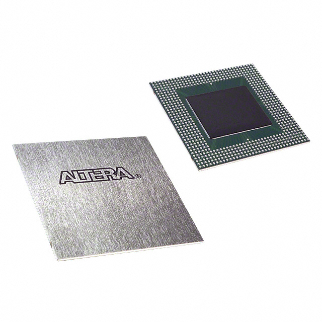
APEX-20KC® Field Programmable Gate Array (FPGA) IC 488 327680 38400 652-BGA |
|---|---|
| Quantity | 656 Available (as of June 18, 2026) |

| Product Category | Field Programmable Gate Array (FPGA) |
|---|---|
| Manufacturer | Intel |
| Manufacturing Status | Obsolete |
| Manufacturer Standard Lead Time | Contact Us |
| Datasheet |
Specifications & Environmental
| Device Package | 652-BGA (45x45) | Grade | Commercial | Operating Temperature | 0°C – 85°C | ||
|---|---|---|---|---|---|---|---|
| Package / Case | 652-BGA | Number of I/O | 488 | Voltage | 1.71 V - 1.89 V | ||
| Mounting Method | Surface Mount | RoHS Compliance | Unknown | REACH Compliance | REACH Unknown | ||
| Moisture Sensitivity Level | 3 (168 Hours) | Number of LABs/CLBs | 3840 | Number of Logic Elements/Cells | 38400 | ||
| Number of Gates | 1772000 | ECCN | OBSOLETE | HTS Code | 0000.00.0000 | ||
| Qualification | N/A | Total RAM Bits | 327680 |
Overview of EP20K1000CB652C7ES – APEX-20KC® Field Programmable Gate Array (FPGA) IC 488 327680 38400 652-BGA
The EP20K1000CB652C7ES is an APEX-20KC® programmable logic device built on a 0.15-μm all-layer copper-metal fabrication process with MultiCore™ architecture. It provides a high-density FPGA fabric with 38,400 logic elements and embedded memory, targeted at designs requiring substantial logic, on-chip RAM, flexible I/O, and advanced clock management.
With up to 1,772,000 system gates, 488 user I/O pins in a 652-BGA (45×45) package, and support for MultiVolt I/O, this commercial-grade device is suited to applications that need high integration, performance, and low-power operation within a 0 °C to 85 °C operating range.
Key Features
- Core Architecture — MultiCore™ architecture integrating look-up table (LUT) logic and embedded memory, implemented in a 0.15-μm copper-metal process for improved performance and lower power.
- Logic Capacity — 38,400 logic elements supporting up to 1,772,000 system gates for complex programmable logic implementations.
- Embedded Memory — Approximately 0.33 Mbits (327,680 bits) of on-chip RAM usable without reducing available logic resources.
- I/O and Package — 488 user I/O pins in a 652-BGA (45×45) package; MultiVolt I/O support for 1.8 V, 2.5 V, and 3.3 V interfaces (5.0-V tolerance achievable with an external resistor as noted).
- Clock Management — Up to four phase-locked loops (PLLs), a built-in low-skew clock tree, and features such as ClockLock, ClockBoost, and ClockShift for flexible clocking and timing control.
- Memory and External Interface Support — Designed to support high-speed external memories including DDR SDRAM and ZBT SRAM and compliant operation with PCI 3.3-V interfaces (33/66 MHz, 32/64 bits) as described in device documentation.
- Low-Power Operation — 1.8-V internal supply design with copper interconnects and ESBs that include programmable power-saving modes to reduce overall power consumption.
- Commercial Grade & Compliance — Commercial-grade device with RoHS compliance; specified operating temperature range 0 °C to 85 °C and supply voltage 1.71 V to 1.89 V.
- Design Tools — Supported by vendor development tools and megafunction libraries for synthesis, placement, and routing as indicated in the product documentation.
Typical Applications
- High-speed memory interfaces — Implement DDR SDRAM or ZBT SRAM controllers and associated logic using the device's on-chip RAM, abundant logic elements, and high-speed I/O support.
- High-throughput I/O bridging — Use the device for PCI-compatible interfaces and multi-voltage I/O bridging where flexible voltage domains and many user I/Os are required.
- Serial/parallel data processing — Deploy the FPGA for LVDS and other high-speed signaling channels, leveraging dedicated interconnect, carry/cascade chains, and clocking resources for low-latency processing.
- Prototyping and embedded systems — Rapidly prototype complex logic and embedded functions with the integrated LUTs, ESBs, and vendor megafunction support.
Unique Advantages
- High integration density: 38,400 logic elements and up to 1,772,000 system gates enable large, consolidated designs that reduce external component count.
- Significant embedded memory: Approximately 0.33 Mbits of on-chip RAM available without reducing logic resources, simplifying buffer and FIFO implementations.
- Flexible multi-voltage I/O: Native support for 1.8 V, 2.5 V, and 3.3 V interfaces enables seamless integration with a range of peripherals and memory devices.
- Advanced clocking: Up to four PLLs plus ClockLock/ClockBoost/ClockShift features provide precise timing control for complex, multi-clock designs.
- Low-power copper process: 1.8-V internal supply and copper interconnects contribute to reduced power consumption in dense logic designs.
- Commercial availability and compliance: RoHS-compliant, commercial-grade device with documented toolchain and megafunction support to accelerate development.
Why Choose EP20K1000CB652C7ES?
The EP20K1000CB652C7ES combines high logic density, substantial embedded RAM, and flexible I/O in a 652-BGA package, offering a compact platform for complex digital designs. Its MultiCore™ architecture, advanced clocking, and vendor tool support make it well suited for designers building memory interfaces, bridging logic, and high-throughput data paths where integration and predictable timing are priorities.
For development teams and OEMs looking to consolidate functions, reduce board-level components, and rely on a documented FPGA architecture and toolset, this APEX-20KC device provides a scalable, commercially graded option that balances performance, power, and I/O flexibility.
Request a quote or submit an inquiry to get pricing, availability, and technical support information for the EP20K1000CB652C7ES.


Date Founded: 1968
Headquarters: Santa Clara, California, USA
Employees: 130,000+
Revenue: $54.23 Billion
Certifications and Memberships: ISO9001:2015, ISO14001:2015, ISO17025:2017, ISO27001:2022, ISO45001:2018, ISO50001:2018


