
EP20K160ETC144-3
| Part Description |
APEX-20KE® Field Programmable Gate Array (FPGA) IC 88 81920 6400 144-LQFP |
|---|---|
| Quantity | 1,356 Available (as of June 14, 2026) |
| Product Category | Field Programmable Gate Array (FPGA) |
|---|---|
| Manufacturer | Intel |
| Manufacturing Status | Obsolete |
| Manufacturer Standard Lead Time | Contact Us |
| Datasheet |
Specifications & Environmental
| Device Package | 144-TQFP (20x20) | Grade | Commercial | Operating Temperature | 0°C – 85°C | ||
|---|---|---|---|---|---|---|---|
| Package / Case | 144-LQFP | Number of I/O | 88 | Voltage | 1.71 V - 1.89 V | ||
| Mounting Method | Surface Mount | RoHS Compliance | Unknown | REACH Compliance | REACH Unaffected | ||
| Moisture Sensitivity Level | 3 (168 Hours) | Number of LABs/CLBs | 640 | Number of Logic Elements/Cells | 6400 | ||
| Number of Gates | 404000 | ECCN | 3A001A2A | HTS Code | 8542.39.0001 | ||
| Qualification | N/A | Total RAM Bits | 81920 |
Overview of EP20K160ETC144-3 – APEX-20KE FPGA, 6,400 logic elements, 144-LQFP
The EP20K160ETC144-3 is an APEX-20KE family field programmable gate array (FPGA) offered by Intel. It combines a MultiCore architecture that integrates look-up table (LUT) logic and embedded system blocks (ESBs) to support register-heavy and memory-intensive functions.
Designed for commercial embedded applications, this device targets SOPC-style integration, memory interface controllers, and high-performance I/O tasks where on-chip memory, flexible clocking and a compact 144-LQFP package are important.
Key Features
- Core Logic 6,400 logic elements and approximately 404,000 system gates provide mid-range programmable logic capacity for control, glue logic and datapath functions.
- Embedded Memory Approximately 81,920 bits of on-chip RAM implemented in ESBs for FIFOs, dual-port RAM and content-addressable memory (CAM) use.
- I/O Capacity and Flexibility 88 user I/O pins with MultiVolt I/O interface support (family-level) enabling interoperable signaling with 1.8 V, 2.5 V, 3.3 V and 5.0 V domains.
- Advanced Clock Management Family-level support for up to four phase-locked loops (PLLs), up to eight global clocks, and ClockLock/ClockBoost/ClockShift features for programmable clock multiplication, division and phase shifting.
- High-speed I/O Options (family capability) Support for DDR SDRAM and ZBT SRAM interfaces and LVDS signaling capability (family-level LVDS performance up to 840 Mbits per channel).
- Power and Supply Internal supply requirement specified at 1.71 V to 1.89 V for this device; family-level low-power design and programmable ESB power-saving modes.
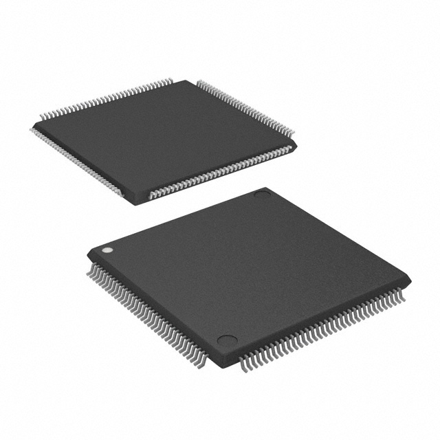
- Package and Mounting 144-LQFP (144-TQFP, 20 × 20) surface-mount package for compact PCB integration.
- Operating Range and Compliance Commercial grade device with an operating temperature range of 0 °C to 85 °C and RoHS-compliant status.
Typical Applications
- PCI and Peripheral Interface Logic Implements bus bridging and custom peripheral interfaces leveraging family-level PCI compliance for 3.3-V operation and high-speed I/O.
- Memory Interface Controllers Acts as a controller or glue logic for DDR SDRAM and ZBT SRAM systems using embedded memory and high-speed I/O support.
- Embedded System Integration (SOPC) Uses ESBs for on-chip FIFOs, dual-port RAM and CAMs to build system-on-a-programmable-chip elements and custom processing blocks.
- Clock- and Timing-Sensitive Designs Employs on-chip PLLs and clock management features for applications requiring phase control, clock multiplication/division and reduced skew.
Unique Advantages
- Balanced Logic Density: 6,400 logic elements provide a mid-range capacity that supports complex control and datapath designs without excessive PCB footprint.
- On-Chip Memory Integration: Approximately 81,920 bits of embedded memory in ESBs enable efficient implementation of FIFOs, buffers and dual-port RAM without external components.
- Flexible I/O: 88 user I/O pins with MultiVolt family-level support allow direct interfacing to multiple voltage domains and external memory devices.
- Robust Clocking: Family-level PLLs, global clock resources and ClockLock/ClockBoost features permit precise clock management for timing-critical systems.
- Compact, Surface-Mount Package: 144-LQFP (20 × 20) surface-mount package facilitates space-constrained board designs while maintaining accessible I/O.
- Commercial-Grade and RoHS Compliant: Rated for 0 °C to 85 °C operation and conformant with RoHS requirements for standard commercial applications.
Why Choose EP20K160ETC144-3?
The EP20K160ETC144-3 combines the APEX-20KE family architecture with a practical mix of logic capacity, embedded memory and I/O flexibility in a compact 144-LQFP package. Its Commercial grade and RoHS compliance make it suitable for a wide range of embedded designs that require integrated memory blocks, configurable clocking and MultiVolt I/O interoperability.
This device is appropriate for engineers building SOPC elements, memory interface controllers, PCI/board-level interfaces and other mid-range FPGA applications where a balance of logic elements, on-chip RAM and advanced clocking features is required.
Request a quote or submit a purchase inquiry to evaluate EP20K160ETC144-3 for your next commercial embedded design project.


Date Founded: 1968
Headquarters: Santa Clara, California, USA
Employees: 130,000+
Revenue: $54.23 Billion
Certifications and Memberships: ISO9001:2015, ISO14001:2015, ISO17025:2017, ISO27001:2022, ISO45001:2018, ISO50001:2018


