
EP20K200BC356-1X
| Part Description |
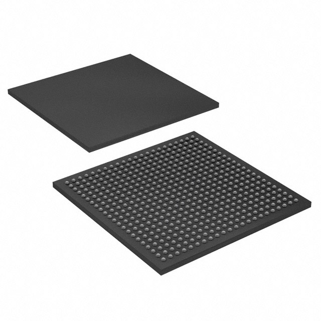
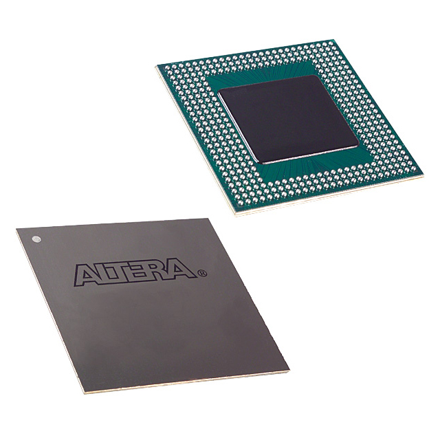
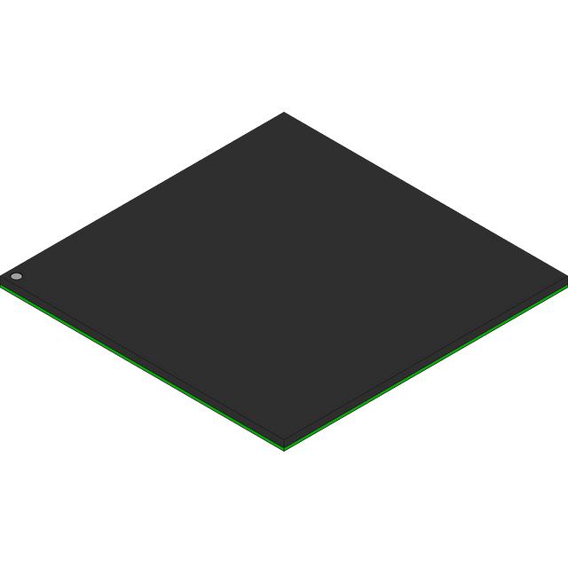
APEX-20K® Field Programmable Gate Array (FPGA) IC 277 106496 8320 356-LBGA |
|---|---|
| Quantity | 1,201 Available (as of June 15, 2026) |

| Product Category | Field Programmable Gate Array (FPGA) |
|---|---|
| Manufacturer | Intel |
| Manufacturing Status | Obsolete |
| Manufacturer Standard Lead Time | Contact Us |
| Datasheet |
Specifications & Environmental
| Device Package | 356-BGA (35x35) | Grade | Commercial | Operating Temperature | 0°C – 85°C | ||
|---|---|---|---|---|---|---|---|
| Package / Case | 356-LBGA | Number of I/O | 277 | Voltage | 2.375 V - 2.625 V | ||
| Mounting Method | Surface Mount | RoHS Compliance | Unknown | REACH Compliance | REACH Unaffected | ||
| Moisture Sensitivity Level | 3 (168 Hours) | Number of LABs/CLBs | 832 | Number of Logic Elements/Cells | 8320 | ||
| Number of Gates | 526000 | ECCN | 3A001A2A | HTS Code | 8542.39.0001 | ||
| Qualification | N/A | Total RAM Bits | 106496 |
Overview of EP20K200BC356-1X – APEX-20K® Field Programmable Gate Array (FPGA) IC 277 106496 8320 356-LBGA
The EP20K200BC356-1X is an APEX-20K family FPGA offered in a 356‑ball LFBGA package. It implements the APEX MultiCore architecture that integrates look-up table (LUT) logic, product‑term logic and embedded memory to support system-on-a-programmable-chip (SOPC) designs.
With 8,320 logic elements, approximately 106,496 bits of embedded RAM, and 277 I/O pins in a compact surface‑mount 35×35 356‑BGA package, this device is targeted at designs requiring mid-range programmable logic density, embedded memory, and flexible I/O and clock management within commercial temperature ratings.
Key Features
- MultiCore architecture Family-level MultiCore architecture combining LUT logic, product‑term logic and embedded system blocks for SOPC integration and mixed logic/memory implementations.
- Logic capacity 8,320 logic elements and a device gate count of 526,000 provide mid-range programmable logic density for control, glue‑logic and function acceleration.
- Embedded memory Approximately 106,496 bits of on‑chip RAM for FIFOs, dual‑port RAM and CAM-style implementations.
- I/O and interface flexibility 277 user I/O pins with MultiVolt I/O interface support and advanced I/O features at the family level, enabling direct connection to a variety of voltage domains and high‑speed external memories.
- Clock management Family features include up to four PLLs, a built‑in low‑skew clock tree, up to eight global clock signals, and programmable clock features such as ClockLock, ClockBoost and ClockShift for fine phase and frequency control.
- Low‑power family features Designed for low‑power operation at the device supply range provided; family-level power-saving modes are available for embedded system blocks.
- Package and mounting Surface-mount 356‑LBGA (35×35) package suitable for space‑efficient board layouts and high pin density.
- Commercial grade and environmental compliance Commercial operating temperature range of 0 °C to 85 °C and RoHS compliant.
Typical Applications
- System-on-a-programmable-chip (SOPC) integration Implement embedded system blocks and combine logic and memory to create custom SOPC solutions.
- High‑speed memory interfaces Support for high‑speed external memory interfaces at the family level makes this FPGA suitable for DDR SDRAM and SRAM controller logic.
- Peripheral and bus bridging Use in designs requiring PCI‑class peripheral interfaces and flexible I/O to bridge between different voltage domains and bus standards.
- High‑throughput serial and differential I/O Leverage family LVDS and high‑speed I/O capabilities for communications and signal‑processing front ends.
Unique Advantages
- Highly integrated MultiCore design: Combines LUTs, product‑term logic and embedded system blocks to reduce external component count and simplify complex functions.
- Balanced density and memory: 8,320 logic elements alongside approximately 106,496 bits of embedded RAM give designers both logic and on‑chip storage for mid‑range applications.
- Flexible I/O resources: 277 I/O pins and family support for MultiVolt interfaces enable mixed‑voltage system integration and direct connections to external devices.
- Advanced clock control: On‑device PLLs and programmable clock features provide deterministic timing and reduced clock skew for synchronized system designs.
- Compact, manufacturable package: 356‑LBGA surface‑mount package offers a high pin count in a compact footprint suitable for production assembly.
- RoHS compliant, commercial grade: Ready for commercial applications across a 0 °C to 85 °C range with environmental compliance for mainstream production.
Why Choose EP20K200BC356-1X?
The EP20K200BC356-1X positions itself as a versatile mid‑density FPGA option within the APEX‑20K family, combining 8,320 logic elements, substantial embedded RAM and broad I/O capacity in a 356‑LBGA package. Its MultiCore architecture and family clock/I/O features make it suitable for designs that require integrated memory, flexible peripheral interfacing, and programmable logic in a commercial‑grade device.
This device is well suited to engineering teams building SOPC solutions, memory interface controllers, peripheral bridges, and high‑speed I/O subsystems where a balance of logic density, on‑chip memory and clock management is required. The combination of package, compliance and operating range supports streamlined integration into production designs.
Request a quote or submit an inquiry to get pricing and availability information for the EP20K200BC356-1X. Engineers and buyers can request detailed procurement information, lead times and volume pricing to support project planning.


Date Founded: 1968
Headquarters: Santa Clara, California, USA
Employees: 130,000+
Revenue: $54.23 Billion
Certifications and Memberships: ISO9001:2015, ISO14001:2015, ISO17025:2017, ISO27001:2022, ISO45001:2018, ISO50001:2018


