
EP20K200FC484-1XN
| Part Description |
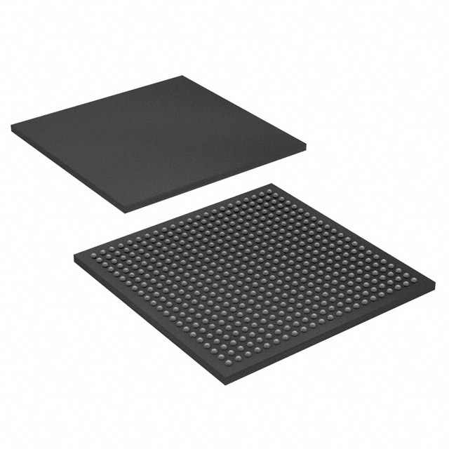
APEX-20K® Field Programmable Gate Array (FPGA) IC 382 106496 8320 484-BBGA |
|---|---|
| Quantity | 955 Available (as of June 10, 2026) |

| Product Category | Field Programmable Gate Array (FPGA) |
|---|---|
| Manufacturer | Intel |
| Manufacturing Status | Obsolete |
| Manufacturer Standard Lead Time | Contact Us |
| Datasheet |
Specifications & Environmental
| Device Package | 484-FBGA (23x23) | Grade | Commercial | Operating Temperature | 0°C – 85°C | ||
|---|---|---|---|---|---|---|---|
| Package / Case | 484-BBGA | Number of I/O | 382 | Voltage | 2.375 V - 2.625 V | ||
| Mounting Method | Surface Mount | RoHS Compliance | Unknown | REACH Compliance | REACH Unaffected | ||
| Moisture Sensitivity Level | 3 (168 Hours) | Number of LABs/CLBs | 832 | Number of Logic Elements/Cells | 8320 | ||
| Number of Gates | 526000 | ECCN | 3A001A2A | HTS Code | 8542.39.0001 | ||
| Qualification | N/A | Total RAM Bits | 106496 |
Overview of EP20K200FC484-1XN – APEX-20K® FPGA, 8,320 logic elements, 106,496-bit RAM, 382 I/O, 484-BBGA
The EP20K200FC484-1XN is an APEX-20K family field programmable gate array (FPGA) from Intel, delivering 8,320 logic elements, 106,496 total RAM bits and 382 user I/O pins in a 484-BBGA package. It implements the APEX 20K MultiCore architecture, combining lookup-table logic, product-term logic and embedded system blocks to enable system-on-a-programmable-chip integration.
Designed for commercial-grade embedded applications, the device supports flexible I/O and clocking features while operating from a 2.375–2.625 V supply and a 0 °C to 85 °C operating range. RoHS compliant and surface-mount packaged, it suits compact, board-mounted FPGA designs requiring moderate gate density and on-chip memory.
Key Features
- Core Capacity – 8,320 logic elements and up to 526,000 system gates provide combinatorial and register resources for custom logic and control functions.
- Embedded Memory – 106,496 total RAM bits of on-chip memory (approximately 0.106 Mbits) for FIFOs, dual-port RAM and other storage implemented in embedded system blocks.
- I/O Density & Flexibility – 382 user I/O pins to drive parallel interfaces and board-level connectivity; supports programmable clamp and per-pin tri-state control as part of the APEX 20K family feature set.
- Package & Mounting – 484-BBGA (supplier package 484-FBGA, 23×23) in a surface-mount form factor to support compact board layouts.
- Power – Voltage supply 2.375 V to 2.625 V aligned with the device’s internal supply requirements; family-level design emphasizes low-power operation and programmable power-saving modes.
- Clocking & Timing – APEX 20K family clock-management features include multiple PLLs, low-skew clock tree and up to eight global clock signals for predictable timing and flexible clock domain control.
- Memory & Bus Support – Family-level support for high-speed external memories (including DDR SDRAM and ZBT SRAM) and compliance options for PCI Local Bus 2.2 at 3.3 V operation (family specification).
- Operating Range & Compliance – Commercial-grade operating temperature from 0 °C to 85 °C and RoHS compliance for global assembly requirements.
Typical Applications
- System Integration / SOPC – Implement embedded controllers, glue logic and integrated subsystems using the MultiCore architecture and on-chip memory blocks to reduce external components.
- Memory Interface Controllers – Build DDR SDRAM or ZBT SRAM controllers and buffering logic using the device’s embedded RAM resources and family-level memory support.
- PCI / Bus Bridging – Deploy in PCI-compliant designs (3.3 V, 33/66 MHz, 32/64-bit modes supported at the family level) for custom bus logic and protocol conversion.
- High-speed I/O & Data Paths – Use the 382 I/O pins and family-supported differential/parallel I/O standards for high-throughput data capture, aggregation and routing.
Unique Advantages
- Highly integrated MultiCore architecture – Combines LUT logic, product-term logic and embedded system blocks to implement both logic and memory functions on-chip, reducing external BOM and board area.
- Substantial embedded RAM – 106,496 total RAM bits enable local buffering and FIFO implementation without sacrificing logic resources.
- Flexible clock management – Family-level PLLs and a low-skew clock tree support multiple clock domains and predictable timing for synchronous designs.
- Versatile I/O capability – High I/O count and family-level MultiVolt interface support simplify interface to a wide range of external devices and voltage domains.
- Commercial operating range with RoHS compliance – Suitable for commercial embedded products requiring standard temperature range operation and environmental compliance for lead-free assembly.
Why Choose EP20K200FC484-1XN?
The EP20K200FC484-1XN positions itself as a mid-density APEX-20K FPGA option, offering a balance of logic capacity (8,320 logic elements), meaningful on-chip memory (106,496 bits) and a high I/O count (382 pins) in a compact 484-BBGA package. Its APEX family architecture enables integrated logic and memory implementations useful for system-on-chip-style designs where reducing external components is important.
This device is well suited to commercial embedded designs that require moderate gate counts, on-board memory resources, flexible clocking and varied I/O, providing a platform that scales with APEX 20K family design methodologies and tool support.
Request a quote or submit an inquiry to obtain pricing, availability and lead-time information for the EP20K200FC484-1XN. Our team can assist with ordering details and supply options.


Date Founded: 1968
Headquarters: Santa Clara, California, USA
Employees: 130,000+
Revenue: $54.23 Billion
Certifications and Memberships: ISO9001:2015, ISO14001:2015, ISO17025:2017, ISO27001:2022, ISO45001:2018, ISO50001:2018


