
EP2AGX260FF35I5N
| Part Description |
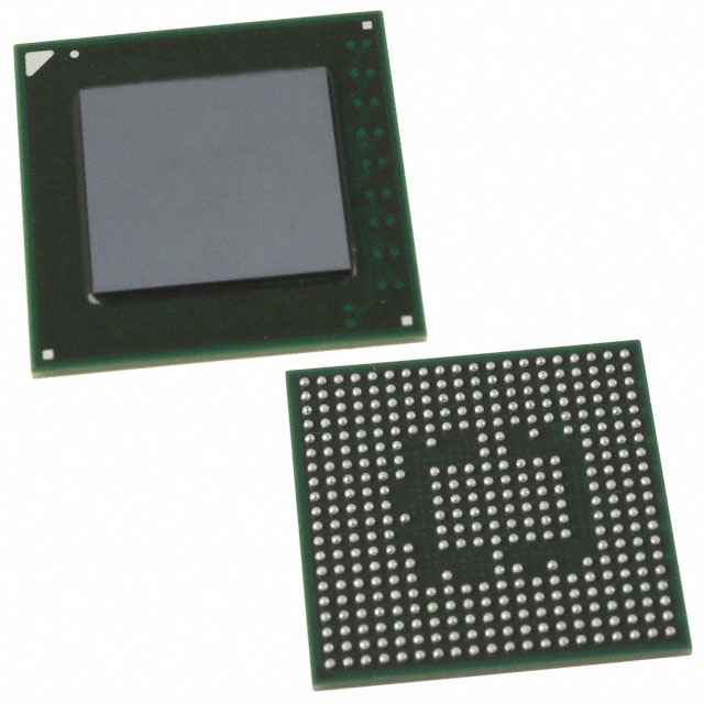
Arria II GX Field Programmable Gate Array (FPGA) IC 612 12038144 244188 1152-BBGA, FCBGA |
|---|---|
| Quantity | 1,222 Available (as of June 15, 2026) |

| Product Category | Field Programmable Gate Array (FPGA) |
|---|---|
| Manufacturer | Intel |
| Manufacturing Status | Obsolete |
| Manufacturer Standard Lead Time | Contact Us |
| Datasheet |
Specifications & Environmental
| Device Package | 1152-FBGA (35x35) | Grade | Industrial | Operating Temperature | -40°C – 100°C | ||
|---|---|---|---|---|---|---|---|
| Package / Case | 1152-BBGA, FCBGA | Number of I/O | 612 | Voltage | 870 mV - 930 mV | ||
| Mounting Method | Surface Mount | RoHS Compliance | RoHS Compliant | REACH Compliance | REACH Unknown | ||
| Moisture Sensitivity Level | 3 (168 Hours) | Number of LABs/CLBs | 10260 | Number of Logic Elements/Cells | 244188 | ||
| Number of Gates | N/A | ECCN | 3A001A7A | HTS Code | 8542.39.0001 | ||
| Qualification | N/A | Total RAM Bits | 12038144 |
Overview of EP2AGX260FF35I5N – Arria II GX Field Programmable Gate Array (FPGA) IC
The EP2AGX260FF35I5N is an Arria II GX FPGA supplied in a 1152-BBGA (FCBGA) surface-mount package and specified as industrial grade. It provides a combination of high logic capacity, on-chip memory, and dense I/O for designs that require substantial programmable logic and flexible interfacing.
Key device characteristics include 244,188 logic elements, approximately 12.04 Mbits of embedded memory, and 612 I/O pins, enabling integration of complex digital, interface, and protocol functions in a single FPGA package.
Key Features
- Core Logic Capacity 244,188 logic elements (logic cells) for implementing large-scale programmable logic and custom datapaths.
- Embedded Memory Approximately 12.04 Mbits of on-chip RAM (12,038,144 bits) to support buffering, FIFOs, and on-chip data storage.
- I/O Density 612 I/O pins to support high pin-count interfaces and multiple parallel or serial connections.
- Programmable I/O and Timing Device documentation covers I/O timing controls including programmable I/O element (IOE) delay and programmable output buffer delay for precise interface tuning.
- Transceiver and PCIe Support (Documented) Datasheet content references transceiver specifications and a PCI Express (PIPE) HIP block, as part of the device’s electrical and switching characteristics.
- Power Core supply voltage range documented at 0.870 V to 0.930 V to guide power-supply design and budgeting.
- Package and Mounting 1152-BBGA, FCBGA package (supplier package: 1152-FBGA, 35×35) with surface-mount mounting for compact, high-density board designs.
- Temperature Range Industrial operating temperature range from −40 °C to 100 °C for deployment in temperature-challenging environments.
- Regulatory RoHS compliant.
Typical Applications
- PCI Express and High-speed Serial Interfaces Device documentation includes transceiver and PCI Express (PIPE) HIP block references, making the device suitable where documented transceiver and PCIe building blocks are required.
- Custom I/O and Protocol Bridging High I/O count and programmable I/O timing support complex interface logic, protocol conversion, and board-level bridging tasks.
- Compute- and Memory-intensive Logic Large logic element count and approximately 12.04 Mbits of embedded memory enable implementation of significant on-chip processing, buffering, and custom data flows.
Unique Advantages
- High Logic Density: 244,188 logic elements provide capacity for large designs and complex state machines without resorting to multiple devices.
- Substantial On-chip Memory: Approximately 12.04 Mbits of embedded RAM reduces reliance on external memory for many buffering and temporary storage needs.
- Extensive I/O Capacity: 612 I/Os permit flexible partitioning between high-speed interfaces and parallel peripheral connections.
- Configured I/O Timing: Programmable IOE and output buffer delays documented in the device handbook allow precise timing adjustment for interfacing varied peripherals.
- Designed for Industrial Use: Specified −40 °C to 100 °C operating range supports deployment in industrial temperature environments.
- Compact, High-density Package: 1152-BBGA (35×35 supplier package) enables high-pin-count capability in a compact footprint.
Why Choose EP2AGX260FF35I5N?
The EP2AGX260FF35I5N delivers a balanced combination of high logic element count, significant embedded memory, and large I/O capacity within a compact 1152-BBGA package. Its documented programmable I/O timing and transceiver/PCIe references in the device handbook make it a fit for engineered solutions that require detailed electrical and switching characterization.
This part is appropriate for development teams and systems integrators who need a single FPGA solution capable of consolidating complex logic, buffering, and multi-interface connectivity while meeting industrial temperature requirements and RoHS compliance.
Request a quote or submit a purchase inquiry to check pricing and availability for EP2AGX260FF35I5N and to discuss how this device can fit into your next design.


Date Founded: 1968
Headquarters: Santa Clara, California, USA
Employees: 130,000+
Revenue: $54.23 Billion
Certifications and Memberships: ISO9001:2015, ISO14001:2015, ISO17025:2017, ISO27001:2022, ISO45001:2018, ISO50001:2018


