
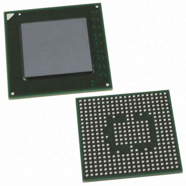
EP2AGX260FF35I5
| Part Description |
Arria II GX Field Programmable Gate Array (FPGA) IC 612 12038144 244188 1152-BBGA, FCBGA |
|---|---|
| Quantity | 1,872 Available (as of October 8, 2026) |

| Product Category | Field Programmable Gate Array (FPGA) |
|---|---|
| Manufacturer | Intel |
| Manufacturing Status | Obsolete |
| Manufacturer Standard Lead Time | Contact Us |
| Datasheet |
Specifications & Environmental
| Device Package | 1152-FBGA (35x35) | Grade | Industrial | Operating Temperature | -40°C – 100°C | ||
|---|---|---|---|---|---|---|---|
| Package / Case | 1152-BBGA, FCBGA | Number of I/O | 612 | Voltage | 870 mV - 930 mV | ||
| Mounting Method | Surface Mount | RoHS Compliance | RoHS non-compliant | REACH Compliance | REACH Unknown | ||
| Moisture Sensitivity Level | 3 (168 Hours) | Number of LABs/CLBs | 10260 | Number of Logic Elements/Cells | 244188 | ||
| Number of Gates | N/A | ECCN | 3A001A7A | HTS Code | 8542.39.0001 | ||
| Qualification | N/A | Total RAM Bits | 12038144 |
Overview of EP2AGX260FF35I5 – Arria II GX Field Programmable Gate Array (FPGA) IC, 244,188 logic elements
The EP2AGX260FF35I5 is an Arria II GX FPGA from Intel offering a high-density programmable fabric for complex digital designs. The device integrates a large logic array alongside on-chip RAM and extensive I/O in a compact FCBGA package.
Designed for applications that require high logic capacity, significant embedded memory, and transceiver-capable peripherals, this industrial-grade device provides the documented electrical and transceiver characteristics found in the Arria II device handbook and device datasheet.
Key Features
- Programmable logic density — 244,188 logic elements to implement complex logic functions and custom hardware accelerators.
- Embedded memory — Total on-chip RAM of 12,038,144 bits (approximately 12 Mbits) to support buffering, LUT-based storage, and state machines without immediate dependence on external memory.
- Extensive I/O — 612 I/O pins for broad connectivity to peripherals, sensors, and high-speed interfaces.
- Transceiver and I/O timing capabilities — Device documentation includes transceiver performance specifications, programmable I/O element delay, and programmable output buffer delay for deterministic I/O timing and serial link support.
- Compact package & mounting — 1152-BBGA (FCBGA) supplier package (1152-FBGA, 35×35) with surface-mount mounting for dense PCB integration.
- Low-voltage core supply — Core voltage supply range of 870 mV to 930 mV to align with modern low-voltage power domains.
- Industrial temperature and grade — Industrial grade device rated for operation from −40 °C to 100 °C for deployment in harsh environments.
- Regulatory compliance — RoHS compliant.
Typical Applications
- High-speed communications — Use where on-chip transceiver performance and PCIe-compatible building blocks are required for serial links and network interfaces.
- Industrial control and automation — Industrial-grade temperature range and wide I/O complement real-time control, data aggregation, and interface consolidation in factory and field systems.
- Embedded systems and custom logic — Large logic capacity and on-chip memory support complex signal processing, control algorithms, and system integration on a single FPGA.
Unique Advantages
- High logic capacity: 244,188 logic elements enable implementation of sizable custom hardware designs and parallel processing architectures.
- Generous on-chip memory: Approximately 12 Mbits of embedded RAM reduces dependency on external memory for many buffering and storage needs.
- Broad I/O connectivity: 612 I/O pins allow dense peripheral interfacing and flexible bank assignments for mixed-signal and digital systems.
- Industrial robustness: Rated for −40 °C to 100 °C operation and offered in an industrial grade package for deployment in demanding environments.
- Efficient core power domain: Narrow core voltage range (0.87–0.93 V) that aligns with low-voltage system designs.
- Board-level integration: 1152-BBGA FCBGA package balances pin count and footprint for compact, high-density PCB layouts.
Why Choose EP2AGX260FF35I5?
The EP2AGX260FF35I5 delivers a balance of high logic density, substantial embedded memory, and extensive I/O in a single industrial-grade Arria II GX device. Its documented transceiver and I/O timing capabilities, combined with the device-level electrical characteristics provided in the Arria II device handbook, make it suitable for designs that require integration of complex digital logic and serial interfaces.
This FPGA is well suited to engineers and system designers building industrial, communications, and embedded systems that demand scalability, deterministic I/O behavior, and a high level of on‑chip integration.
Request a quote or submit an inquiry to begin sourcing EP2AGX260FF35I5 for your next design.

























Date Founded: 1968
Headquarters: Santa Clara, California, USA
Employees: 130,000+
Revenue: $54.23 Billion
Certifications and Memberships: ISO9001:2015, ISO14001:2015, ISO17025:2017, ISO27001:2022, ISO45001:2018, ISO50001:2018


