
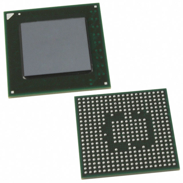
EP2AGX65CU17C4G
| Part Description |
Arria II GX Field Programmable Gate Array (FPGA) IC 156 5371904 60214 358-LFBGA, FCBGA |
|---|---|
| Quantity | 811 Available (as of October 7, 2026) |

| Product Category | Field Programmable Gate Array (FPGA) |
|---|---|
| Manufacturer | Intel |
| Manufacturing Status | Active |
| Manufacturer Standard Lead Time | 26 Weeks |
| Datasheet |
Specifications & Environmental
| Device Package | 358-UBGA, FCBGA (17x17) | Grade | Commercial | Operating Temperature | 0°C – 85°C | ||
|---|---|---|---|---|---|---|---|
| Package / Case | 358-LFBGA, FCBGA | Number of I/O | 156 | Voltage | 870 mV - 930 mV | ||
| Mounting Method | Surface Mount | RoHS Compliance | RoHS Compliant | REACH Compliance | REACH Unaffected | ||
| Moisture Sensitivity Level | 3 (168 Hours) | Number of LABs/CLBs | 2530 | Number of Logic Elements/Cells | 60214 | ||
| Number of Gates | N/A | ECCN | 3A991D | HTS Code | 8542.39.0001 | ||
| Qualification | N/A | Total RAM Bits | 5371904 |
Overview of EP2AGX65CU17C4G – Arria II GX Field Programmable Gate Array (FPGA) IC 156 5371904 60214 358-LFBGA, FCBGA
The EP2AGX65CU17C4G is an Intel Arria II GX FPGA in a 358‑LFBGA (358‑UBGA / FCBGA, 17 × 17) surface‑mount package. It delivers a mid‑range FPGA resource set for designs that require a balance of programmable logic, on‑chip memory and flexible I/O.
Built on the Arria II device family architecture, the device targets applications that need integrated high‑performance DSP and serial/parallel interfaces, offering designers a combination of logic density, embedded memory and IO count for edge networking, communications and signal processing tasks.
Key Features
- Logic Capacity — 60,214 logic elements (cells) to implement combinational and sequential logic in FPGA designs.
- Embedded Memory — Approximately 5.37 Mbits of on‑chip RAM for FIFOs, buffers and local data storage.
- I/O Count — 156 user I/O pins suitable for multiple parallel interfaces and peripheral connections.
- Power and Supply — Operates from a core voltage supply range of 870 mV to 930 mV to support optimized power domains.
- Operating Range — Commercial temperature grade with specified operation from 0 °C to 85 °C.
- Package and Mounting — 358‑LFBGA / 358‑UBGA FCBGA package, 17 × 17; surface mount for PCB integration.
- Environmental Compliance — RoHS compliant.
- Arria II Family Capabilities — Family features include a 40‑nm low‑power FPGA engine, adaptive logic modules (ALMs) with eight‑input fracturable LUTs, dedicated DSP blocks (family‑level DSP performance up to 550 MHz), and integrated hard IP and SERDES/transceiver support for common serial protocols and high‑bandwidth links (family‑level transceiver rates up to 6.375 Gbps and support for protocols such as PCIe, Ethernet and DDR3 as documented for the Arria II family).
Typical Applications
- High‑speed serial communications — Implement protocol bridging, packet processing and SERDES‑based links using the Arria II family transceiver capabilities.
- Networking & Telecom — Use the device’s logic density, embedded memory and I/O to support switch, router or baseband processing functions.
- Signal processing / DSP — Leverage family DSP resources and on‑chip RAM for filtering, FFTs and other real‑time signal operations.
- Memory interfaces & buffering — Combine on‑chip RAM and I/O to create DDR3 interfaces, data buffering, and traffic management functions (Arria II family supports DDR3 integration as part of device interfaces).
Unique Advantages
- Balanced resource footprint: 60,214 logic elements with ~5.37 Mbits of embedded memory provides a practical mix of logic and storage for mid‑range FPGA designs.
- Family‑level interface integration: Arria II family features for high‑speed serial protocols and PHY/MAC hard IP reduce design integration time for common interfaces.
- Commercial temperature suitability: Rated for 0 °C to 85 °C operation to match a wide range of commercial applications and deployment environments.
- Compact FCBGA package: 358‑pin LFBGA / UBGA (17 × 17) surface‑mount footprint simplifies PCB layout for space‑constrained boards.
- Power domain control: Core supply range (870–930 mV) enables designers to align power planning with system requirements.
- Regulatory readiness: RoHS compliance supports modern electronic manufacturing and environmental requirements.
Why Choose EP2AGX65CU17C4G?
The EP2AGX65CU17C4G combines a well‑balanced set of programmable logic, embedded memory and I/O in an Arria II GX family device, making it suitable for engineers developing mid‑range communications, networking and DSP‑centric designs. Its family heritage provides documented support for high‑speed serial protocols, DSP building blocks and common system interfaces to accelerate integration.
This part is appropriate for designs that need roughly 60k logic elements, several megabits of on‑chip RAM, and a 156‑pin I/O complement in a compact FCBGA package—providing scalability and ecosystem support that align with long‑term product development and maintenance.
Request a quote or submit a procurement inquiry to receive availability and pricing details for EP2AGX65CU17C4G.
























Date Founded: 1968
Headquarters: Santa Clara, California, USA
Employees: 130,000+
Revenue: $54.23 Billion
Certifications and Memberships: ISO9001:2015, ISO14001:2015, ISO17025:2017, ISO27001:2022, ISO45001:2018, ISO50001:2018


