
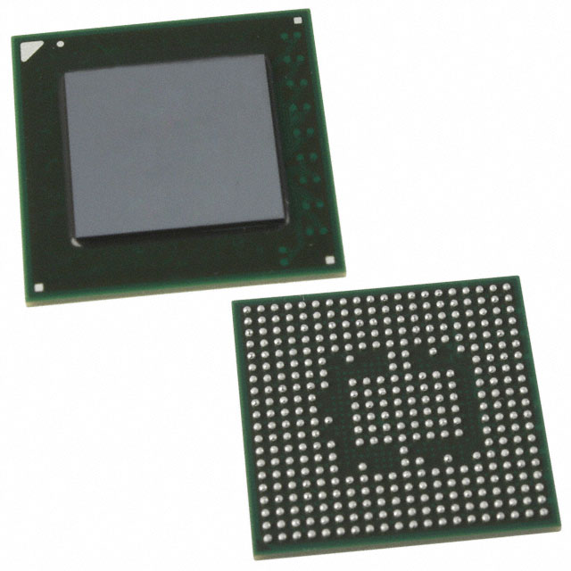
EP2AGX65CU17C6G
| Part Description |
Arria II GX Field Programmable Gate Array (FPGA) IC 156 5371904 60214 358-LFBGA, FCBGA |
|---|---|
| Quantity | 1,298 Available (as of June 18, 2026) |

| Product Category | Field Programmable Gate Array (FPGA) |
|---|---|
| Manufacturer | Intel |
| Manufacturing Status | Active |
| Manufacturer Standard Lead Time | 26 Weeks |
| Datasheet |
Specifications & Environmental
| Device Package | 358-UBGA, FCBGA (17x17) | Grade | Commercial | Operating Temperature | 0°C – 85°C | ||
|---|---|---|---|---|---|---|---|
| Package / Case | 358-LFBGA, FCBGA | Number of I/O | 156 | Voltage | 870 mV - 930 mV | ||
| Mounting Method | Surface Mount | RoHS Compliance | RoHS Compliant | REACH Compliance | REACH Unaffected | ||
| Moisture Sensitivity Level | 3 (168 Hours) | Number of LABs/CLBs | 2530 | Number of Logic Elements/Cells | 60214 | ||
| Number of Gates | N/A | ECCN | PENDING ECCN | HTS Code | 0000.00.0000 | ||
| Qualification | N/A | Total RAM Bits | 5371904 |
Overview of EP2AGX65CU17C6G – Arria II GX FPGA, 358-LFBGA
The EP2AGX65CU17C6G is an Intel Arria II GX Field Programmable Gate Array (FPGA) in a 358-LFBGA FCBGA package intended for commercial applications. It provides a balance of configurable logic, embedded memory, and I/O density for system designs that require on-chip programmability and integration.
This device delivers approximately 60,214 logic elements, approximately 5.37 Mbits of embedded memory, and support for up to 156 I/O signals, making it suitable for designs that need moderate logic capacity, embedded RAM, and flexible connectivity within a compact surface-mount BGA footprint.
Key Features
- Programmable Logic Capacity Approximately 60,214 logic elements for implementing custom digital logic and state machines.
- Embedded Memory Approximately 5.37 Mbits of on-chip RAM to support buffering, FIFO structures, and local data storage.
- I/O Support Up to 156 general-purpose I/O pins to interface with external peripherals and buses.
- Package and Mounting 358-LFBGA (FCBGA) package, supplier device package 358-UBGA (17×17), designed for surface-mount PCB assembly.
- Power Supply Range Core voltage supply range of 870 mV–930 mV for device power planning and regulator selection.
- Operating Temperature Commercial temperature range of 0 °C to 85 °C for typical commercial-environment deployments.
- Compliance RoHS compliant to meet common environmental regulatory requirements.
Typical Applications
- Embedded Systems & Prototyping Implement and iterate custom logic and interfaces using the device’s logic elements and embedded memory.
- Communications & Networking Provide configurable protocol handling and I/O aggregation with up to 156 user I/Os and on-chip RAM.
- Video & Imaging Support intermediate buffering and custom processing pipelines using available embedded memory and logic resources.
- Test & Measurement Enable flexible signal conditioning, counting, and data capture functions leveraging the device’s I/O and memory capabilities.
Unique Advantages
- Right-sized Logic Capacity: Approximately 60,214 logic elements provide a mid-range fabric for designs that need significant but not extreme gate count.
- On-chip Memory Integration: Approximately 5.37 Mbits of embedded RAM reduces reliance on external memory for buffering and local storage.
- Flexible I/O Count: 156 I/Os enable multiple peripheral interfaces and board-level connectivity options without excessive external components.
- Compact BGA Package: 358-LFBGA (17×17) FCBGA footprint supports high-density board layouts while remaining surface-mount compatible.
- Commercial Operating Range: Rated 0 °C to 85 °C for standard commercial applications where that temperature window is appropriate.
- Regulatory Compliance: RoHS compliance supports environmentally conscious product requirements.
Why Choose EP2AGX65CU17C6G?
The EP2AGX65CU17C6G Arria II GX FPGA offers a balanced combination of logic capacity, embedded memory, and I/O density in a compact FCBGA package. Its specification set—approximately 60,214 logic elements, approximately 5.37 Mbits of on-chip RAM, 156 I/Os, and a 358-LFBGA package—makes it well-suited for commercial designs that require configurable logic and local memory without moving to larger device families.
Designed and manufactured by Intel, this device is appropriate for engineers and teams building medium-complexity digital systems, communications interfaces, video processing modules, and test equipment where on-chip integration and a commercial temperature range meet project requirements.
Request a quote or submit a purchase inquiry for the EP2AGX65CU17C6G to receive pricing and availability for your next design.


Date Founded: 1968
Headquarters: Santa Clara, California, USA
Employees: 130,000+
Revenue: $54.23 Billion
Certifications and Memberships: ISO9001:2015, ISO14001:2015, ISO17025:2017, ISO27001:2022, ISO45001:2018, ISO50001:2018


