
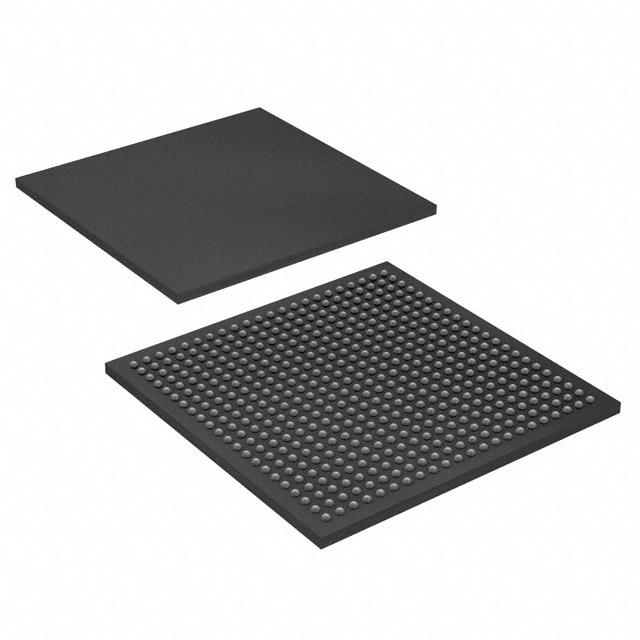
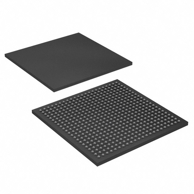
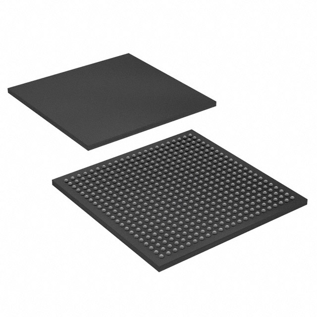
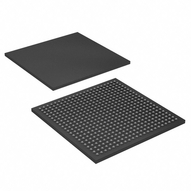
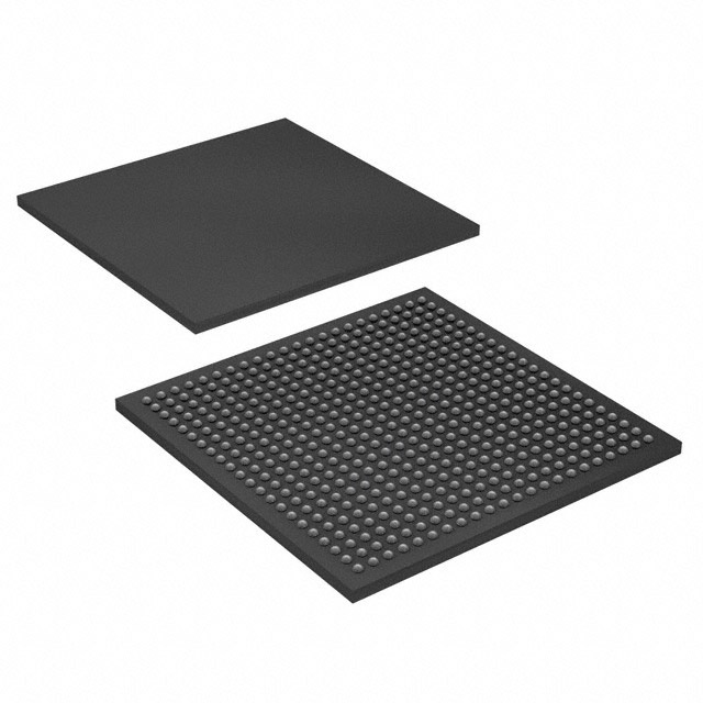
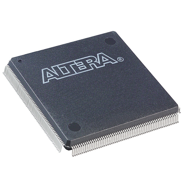
EP2C20F484C8N
| Part Description |
Cyclone® II Field Programmable Gate Array (FPGA) IC 315 239616 18752 484-BGA |
|---|---|
| Quantity | 334 Available (as of October 8, 2026) |
| Product Category | Field Programmable Gate Array (FPGA) |
|---|---|
| Manufacturer | Intel |
| Manufacturing Status | Active |
| Manufacturer Standard Lead Time | 26 Weeks |
| Datasheet |
Specifications & Environmental
| Device Package | 484-FBGA (23x23) | Grade | Commercial | Operating Temperature | 0°C – 85°C | ||
|---|---|---|---|---|---|---|---|
| Package / Case | 484-BGA | Number of I/O | 315 | Voltage | 1.15 V - 1.25 V | ||
| Mounting Method | Surface Mount | RoHS Compliance | RoHS Compliant | REACH Compliance | REACH Unaffected | ||
| Moisture Sensitivity Level | 3 (168 Hours) | Number of LABs/CLBs | 1172 | Number of Logic Elements/Cells | 18752 | ||
| Number of Gates | N/A | ECCN | 3A991D | HTS Code | 8542.39.0001 | ||
| Qualification | N/A | Total RAM Bits | 239616 |
Overview of EP2C20F484C8N – Cyclone® II Field Programmable Gate Array (FPGA) IC 315 239616 18752 484-BGA
The EP2C20F484C8N is a Cyclone® II series field programmable gate array (FPGA) optimized for low-cost embedded processing and DSP-focused solutions. It provides a balance of logic capacity, on-chip memory, and flexible I/O to address medium-density logic and interface tasks in commercial applications.
With 18,752 logic elements, approximately 0.24 Mbits of embedded memory, and 315 general-purpose I/Os in a 484-ball BGA package, this device targets designs that require substantial programmable logic, plentiful I/O, and configurable clocking and memory resources.
Key Features
- Core Logic Provides 18,752 logic elements for implementing combinational and sequential logic, state machines, and custom datapaths.
- Embedded Memory Approximately 0.24 Mbits of on-chip RAM organized for embedded memory use and external-memory interfacing as described in device documentation.
- I/O Density 315 I/O pins support diverse peripheral and bus connections for system integration and high-density interface requirements.
- Clocking and PLLs Includes a global clock network and phase-locked loop (PLL) features for flexible clock distribution and clock management (series-level feature).
- Advanced I/O Features Series documentation notes support for programmable drive strength, slew-rate control, bus-hold, programmable pull-ups, and series on-chip termination for robust I/O integration.
- Embedded DSP Support Cyclone II family architecture includes embedded multipliers and DSP-oriented features suitable for low-cost DSP solutions (series-level feature).
- Power and Package Operates from a core supply of 1.15 V to 1.25 V and is supplied in a 484-FBGA (23×23) surface-mount package (484-BGA case) for compact board-level integration.
- Commercial Grade & Compliance Rated for commercial operating temperatures (0 °C to 85 °C) and RoHS compliant for regulatory conformance.
Typical Applications
- Embedded Processing Low-cost embedded controllers and system logic that leverage the Cyclone II architecture for control, glue logic, and protocol handling.
- DSP and Signal Processing Signal-processing and filtering tasks that use the device’s embedded multipliers and memory resources for efficient datapath implementation.
- Memory Interface Controllers External memory interfacing and buffering functions supported by on-chip memory and documented external-memory interfacing guidance.
- High-Density I/O Bridging Applications requiring many general-purpose I/Os for peripheral aggregation, bus bridging, or multi-device interconnects benefit from the 315 I/O pins.
Unique Advantages
- Substantial Logic Capacity: 18,752 logic elements provide ample programmable resources for medium-complexity designs without external ASIC development.
- Integrated Memory Resources: Approximately 0.24 Mbits of embedded RAM reduces external memory dependence and simplifies board-level BOM.
- High I/O Count: 315 I/Os enable flexible interfacing to sensors, peripherals, and external devices, minimizing the need for additional I/O expanders.
- Flexible Clocking: Global clock network and PLL support provide configurable clock distribution for synchronized multi-domain designs.
- Compact Surface-Mount Package: The 484-FBGA (23×23) package balances pin count and board space for dense system designs.
- Commercial Temperature & RoHS Compliance: Designed for commercial environments (0 °C to 85 °C) and RoHS compliant for regulatory alignment.
Why Choose EP2C20F484C8N?
The EP2C20F484C8N positions itself as a versatile, mid-range Cyclone II FPGA offering a strong combination of logic capacity, embedded memory, and I/O density in a compact 484-BGA package. It is well suited for commercial embedded systems and DSP-focused designs that require on-chip resources for performance and integration.
Engineers and procurement teams looking for a proven Cyclone II device will find this part delivers scalable logic and I/O for medium-complexity applications, backed by comprehensive device documentation and family-level features for clocking, I/O configuration, and memory interfacing.
Request a quote or submit an inquiry to get pricing and availability for the EP2C20F484C8N for your next design.





















Date Founded: 1968
Headquarters: Santa Clara, California, USA
Employees: 130,000+
Revenue: $54.23 Billion
Certifications and Memberships: ISO9001:2015, ISO14001:2015, ISO17025:2017, ISO27001:2022, ISO45001:2018, ISO50001:2018


