
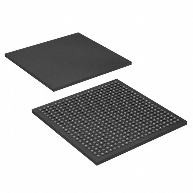
EP2C35F484C7
| Part Description |
Cyclone® II Field Programmable Gate Array (FPGA) IC 322 483840 33216 484-BGA |
|---|---|
| Quantity | 394 Available (as of June 15, 2026) |
| Product Category | Field Programmable Gate Array (FPGA) |
|---|---|
| Manufacturer | Intel |
| Manufacturing Status | Active |
| Manufacturer Standard Lead Time | 26 Weeks |
| Datasheet |
Specifications & Environmental
| Device Package | 484-FBGA (23x23) | Grade | Commercial | Operating Temperature | 0°C – 85°C | ||
|---|---|---|---|---|---|---|---|
| Package / Case | 484-BGA | Number of I/O | 322 | Voltage | 1.15 V - 1.25 V | ||
| Mounting Method | Surface Mount | RoHS Compliance | RoHS non-compliant | REACH Compliance | REACH Unaffected | ||
| Moisture Sensitivity Level | 3 (168 Hours) | Number of LABs/CLBs | 2076 | Number of Logic Elements/Cells | 33216 | ||
| Number of Gates | N/A | ECCN | 3A991D | HTS Code | 8542.39.0001 | ||
| Qualification | N/A | Total RAM Bits | 483840 |
Overview of EP2C35F484C7 – Cyclone® II FPGA, 33,216 logic elements, 484-BGA
The EP2C35F484C7 is a Cyclone® II field-programmable gate array (FPGA) in a 484-ball BGA package designed for commercial embedded and DSP-oriented applications. It integrates 33,216 logic elements, approximately 0.48 Mbits of embedded memory, and a rich I/O fabric with 322 I/O pins to support mid-density programmable logic designs that require flexible I/O and on-chip resources.
With a documented device architecture that includes embedded multipliers, dedicated clock networks and PLLs, and M4K-style memory blocks, this device targets cost-sensitive embedded processing and low-cost DSP solutions while operating from a 1.15 V–1.25 V core supply and an operating temperature range of 0 °C to 85 °C.
Key Features
- Core Logic 33,216 logic elements provide the programmable fabric for implementing custom logic, state machines, and control functions.
- Embedded Memory Approximately 0.48 Mbits of on-chip RAM organized as M4K blocks for efficient storage of buffers, FIFOs, and small data structures.
- DSP-Friendly Resources Architecture-level support for embedded multipliers and DSP-oriented routing and modes, enabling efficient arithmetic and signal-processing implementations.
- I/O Capacity & Flexibility 322 available I/O pins with advanced I/O structure and multi-voltage I/O bank capabilities described in the Cyclone II documentation for interfacing to a wide range of peripherals and external memory.
- Clocking & Timing Dedicated global clock networks and phase-locked loops (PLLs) support complex clocking schemes and low-skew distribution across the device.
- Power & Supply Core voltage supply range of 1.15 V to 1.25 V, with device-level guidance and operating conditions defined in the Cyclone II handbook.
- Package & Mounting Surface-mount 484-ball BGA (484-FBGA, 23×23) package for compact board-level integration.
- Commercial Grade & Compliance Commercial temperature rating (0 °C to 85 °C) and RoHS compliant for standard electronics manufacturing.
Typical Applications
- Embedded Processing Implement control logic, soft processors or embedded peripherals using the device’s logic elements and on-chip memory.
- Low-Cost DSP Deploy signal-processing functions and multiply-accumulate operations leveraging the device’s embedded multipliers and DSP routing.
- I/O Bridging and Protocol Conversion Use the extensive I/O resources and programmable fabric to implement interface bridging, protocol translation, and glue logic between subsystems.
- Prototyping and System Integration Integrate custom logic, timing control and memory buffering in compact BGA form factors for board-level prototypes or volume designs.
Unique Advantages
- Substantial Logic Density: 33,216 logic elements give designers room to implement complex state machines, custom accelerators, and glue logic without external chips.
- On-chip Memory Efficiency: Approximately 0.48 Mbits of embedded RAM (M4K blocks) reduces the need for external memory for many buffering and control tasks.
- DSP-Oriented Resources: Architecture-level inclusion of embedded multipliers simplifies arithmetic-heavy functions and keeps data paths on-chip for lower latency.
- Comprehensive Clocking: Dedicated global clock networks and PLL support enable flexible clock domain management and low-skew distribution across designs.
- High I/O Count in Compact Package: 322 I/O pins in a 484-BGA (23×23) footprint balance board space and I/O connectivity for densely routed designs.
- Manufacturing-Ready Packaging: Surface-mount 484-FBGA package and RoHS compliance align with modern assembly processes and environmental requirements.
Why Choose EP2C35F484C7?
The EP2C35F484C7 provides a balanced mid-range FPGA solution for designers seeking a combination of programmable logic capacity, embedded memory, DSP resources and a high I/O count in a compact BGA package. Its Cyclone II architecture—documented for global clocking, PLLs, embedded multipliers and M4K memory—supports a wide range of embedded and signal-processing tasks while operating within a standard commercial temperature range.
This device suits teams building cost-aware systems that require on-chip arithmetic, flexible I/O interfacing and integrated memory, offering scalability within designs that leverage the Cyclone II feature set and vendor documentation for implementation guidance.
Request a quote or submit a purchase inquiry to get pricing and availability for EP2C35F484C7.


Date Founded: 1968
Headquarters: Santa Clara, California, USA
Employees: 130,000+
Revenue: $54.23 Billion
Certifications and Memberships: ISO9001:2015, ISO14001:2015, ISO17025:2017, ISO27001:2022, ISO45001:2018, ISO50001:2018


