
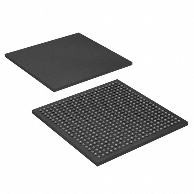
EP2C35F484I8
| Part Description |
Cyclone® II Field Programmable Gate Array (FPGA) IC 322 483840 33216 484-BGA |
|---|---|
| Quantity | 1,624 Available (as of June 15, 2026) |

| Product Category | Field Programmable Gate Array (FPGA) |
|---|---|
| Manufacturer | Intel |
| Manufacturing Status | Active |
| Manufacturer Standard Lead Time | 26 Weeks |
| Datasheet |
Specifications & Environmental
| Device Package | 484-FBGA (23x23) | Grade | Industrial | Operating Temperature | -40°C – 100°C | ||
|---|---|---|---|---|---|---|---|
| Package / Case | 484-BGA | Number of I/O | 322 | Voltage | 1.15 V - 1.25 V | ||
| Mounting Method | Surface Mount | RoHS Compliance | RoHS non-compliant | REACH Compliance | REACH Unaffected | ||
| Moisture Sensitivity Level | 3 (168 Hours) | Number of LABs/CLBs | 2076 | Number of Logic Elements/Cells | 33216 | ||
| Number of Gates | N/A | ECCN | 3A991D | HTS Code | 8542.39.0001 | ||
| Qualification | N/A | Total RAM Bits | 483840 |
Overview of EP2C35F484I8 – Cyclone® II FPGA, 33,216 Logic Elements, 484-FBGA
The EP2C35F484I8 is an Intel Cyclone® II field programmable gate array (FPGA) supplied in a 484-FBGA (23×23) surface-mount package. It implements 33,216 logic elements, approximately 0.48 Mbits of embedded memory, and up to 322 general-purpose I/O pins, making it suited for embedded processing and DSP-oriented implementations within temperature-critical environments.
Built on the Cyclone II architecture, the device provides on-chip memory blocks, embedded multipliers, configurable clocking and PLL resources, and industry-standard configuration and test support—features that target low-cost embedded processing and DSP solutions where integration and predictable electrical characteristics matter.
Key Features
- Logic Capacity 33,216 logic elements to implement complex combinational and sequential logic functions in a single FPGA.
- Embedded Memory Approximately 0.48 Mbits of on-chip RAM (483,840 bits) for data buffering, FIFOs, and small block storage.
- I/O Density Up to 322 I/O pins to support broad interfacing requirements and multiple I/O banks.
- Power Supply Core supply range of 1.15 V to 1.25 V for the FPGA core voltage requirements.
- Package & Mounting 484-FBGA (23×23) package in a surface-mount form factor for compact board-level integration.
- Operating Range & Grade Industrial-grade operation from −40 °C to 100 °C for demanding thermal environments.
- Configuration & Test Cyclone II family support for IEEE Std. 1149.1 (JTAG) boundary scan and configuration options described in the Cyclone II device handbook.
- Architectural Blocks Cyclone II architecture includes global clock networks, PLLs, embedded multipliers, and M4K memory blocks to support common FPGA design patterns.
- RoHS Compliance Device is RoHS compliant for regulatory and manufacturing compatibility.
Typical Applications
- Embedded Processing Low-cost embedded processing functions where on-chip logic and memory reduce external components and simplify system design.
- DSP Acceleration Low-cost DSP solutions leveraging embedded multipliers and local memory for signal processing tasks.
- High-Speed I/O and Memory Interfaces External memory interfacing and high-speed differential I/O implementations that use the Cyclone II I/O structure and multi-bank routing.
- Industrial Control Control and automation applications requiring industrial temperature operation and a high count of I/Os for sensors and actuators.
Unique Advantages
- High Logic Integration: 33,216 logic elements enable consolidation of multiple functions into a single device, reducing board-level complexity.
- On-Chip Memory Resources: Approximately 0.48 Mbits of embedded RAM supports buffering and local storage without adding external memory.
- Generous I/O Count: 322 I/O pins provide flexibility for parallel interfaces, GPIO expansion, and multi-bank signaling.
- Industry Temperature Capability: Rated from −40 °C to 100 °C for deployment in thermally demanding industrial environments.
- Architectural Flexibility: Cyclone II features such as PLLs, global clock networks, embedded multipliers, and M4K memory blocks support diverse design architectures.
- Compact, Surface-Mount Package: 484-FBGA (23×23) enables dense PCB layout while maintaining robust electrical performance.
Why Choose EP2C35F484I8?
The EP2C35F484I8 positions itself as a practical Cyclone II FPGA option where substantial logic capacity, on-chip memory, and a high I/O count are required in a compact 484-FBGA package. Its industrial operating temperature range and RoHS compliance make it suitable for long-term deployment in embedded and industrial systems that rely on predictable supply and thermal characteristics.
Designers targeting low-cost embedded processing, DSP acceleration, and complex I/O interfacing can leverage the Cyclone II architecture—including configurable clocking, embedded multipliers, and M4K memory blocks—to simplify designs, reduce component count, and accelerate development cycles while relying on Intel’s documented device family features.
Request a quote or submit a product inquiry today to obtain pricing and availability information for the EP2C35F484I8.


Date Founded: 1968
Headquarters: Santa Clara, California, USA
Employees: 130,000+
Revenue: $54.23 Billion
Certifications and Memberships: ISO9001:2015, ISO14001:2015, ISO17025:2017, ISO27001:2022, ISO45001:2018, ISO50001:2018


